A 4-layer PCB offers superior signal integrity and reduced electromagnetic interference compared to a 2-layer PCB, making it ideal for complex hardware designs requiring stable performance. The additional layers provide dedicated ground and power planes that enhance power distribution and minimize crosstalk between traces. While 2-layer PCBs are cost-effective for simpler circuits, 4-layer PCBs deliver improved reliability and efficiency in high-speed and high-density hardware engineering applications.
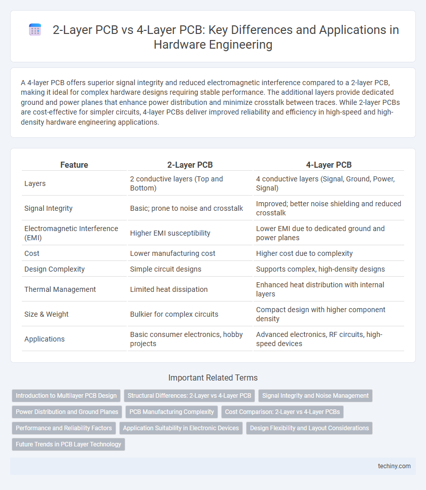
Table of Comparison
| Feature | 2-Layer PCB | 4-Layer PCB |
|---|---|---|
| Layers | 2 conductive layers (Top and Bottom) | 4 conductive layers (Signal, Ground, Power, Signal) |
| Signal Integrity | Basic; prone to noise and crosstalk | Improved; better noise shielding and reduced crosstalk |
| Electromagnetic Interference (EMI) | Higher EMI susceptibility | Lower EMI due to dedicated ground and power planes |
| Cost | Lower manufacturing cost | Higher cost due to complexity |
| Design Complexity | Simple circuit designs | Supports complex, high-density designs |
| Thermal Management | Limited heat dissipation | Enhanced heat distribution with internal layers |
| Size & Weight | Bulkier for complex circuits | Compact design with higher component density |
| Applications | Basic consumer electronics, hobby projects | Advanced electronics, RF circuits, high-speed devices |
Introduction to Multilayer PCB Design
Multilayer PCB design enhances circuit complexity and performance by stacking multiple layers of conductive traces separated by insulating material, enabling compact and efficient layouts. A 2-layer PCB offers limited routing options with one signal and one ground layer, suitable for simple circuits, while a 4-layer PCB incorporates two signal layers and dedicated ground and power planes, improving signal integrity and reducing electromagnetic interference. The additional layers in 4-layer PCBs support advanced hardware engineering requirements by facilitating better power distribution, noise reduction, and higher circuit density.
Structural Differences: 2-Layer vs 4-Layer PCB
A 2-layer PCB consists of two conductive copper layers separated by an insulating substrate, enabling basic circuit designs with limited routing capabilities. In contrast, a 4-layer PCB incorporates four copper layers, typically arranged as signal, ground, power, and another signal layer, providing enhanced signal integrity and reduced electromagnetic interference (EMI). The increased layer count in a 4-layer PCB allows for more complex circuit layouts, improved thermal management, and better overall structural stability compared to a 2-layer PCB.
Signal Integrity and Noise Management
A 4-layer PCB significantly improves signal integrity and noise management compared to a 2-layer PCB by incorporating dedicated ground and power planes, which reduce electromagnetic interference and provide stable reference voltages. The additional layers enable controlled impedance routing and minimize crosstalk, enhancing high-speed signal performance and reducing signal degradation. These advantages make 4-layer PCBs essential in complex hardware designs where clean signal transmission and noise reduction are critical.
Power Distribution and Ground Planes
A 4-layer PCB offers superior power distribution and grounding compared to a 2-layer PCB by incorporating dedicated planes for power and ground, which reduces impedance and minimizes electrical noise. The separated power and ground planes in 4-layer designs provide consistent voltage levels and improve signal integrity, critical for high-speed hardware engineering applications. In contrast, 2-layer PCBs rely on traces for power distribution, often leading to increased inductance and susceptibility to electromagnetic interference (EMI).
PCB Manufacturing Complexity
Manufacturing complexity increases significantly from 2-layer to 4-layer PCBs due to additional lamination steps and precise alignment of internal layers. Four-layer PCBs require advanced fabrication processes such as controlled impedance and impedance matching, which are less critical in two-layer boards. The added layers also necessitate more intricate drilling and plating techniques, leading to higher production costs and longer turnaround times.
Cost Comparison: 2-Layer vs 4-Layer PCBs
2-layer PCBs generally offer a lower cost due to simpler manufacturing processes, making them ideal for budget-sensitive and less complex electronic designs. In contrast, 4-layer PCBs, though more expensive, provide enhanced electrical performance, improved signal integrity, and better EMI shielding, justifying their higher production costs in advanced applications. When balancing cost and functionality, 2-layer PCBs suit basic projects, whereas 4-layer PCBs are preferred for sophisticated devices requiring reliable multilayer routing.
Performance and Reliability Factors
A 4-layer PCB offers superior signal integrity and reduced electromagnetic interference compared to a 2-layer PCB, enhancing overall performance in complex hardware designs. The additional power and ground planes in a 4-layer PCB improve voltage stability and thermal dissipation, increasing reliability under high-frequency and high-power conditions. In contrast, 2-layer PCBs may face limitations in noise reduction and mechanical robustness, making them less suitable for advanced hardware engineering applications requiring consistent electrical performance.
Application Suitability in Electronic Devices
2-layer PCBs are ideal for simple electronic devices and prototypes with low component density, offering cost-effective solutions for consumer electronics and basic control systems. 4-layer PCBs provide enhanced signal integrity and electromagnetic compatibility, making them suitable for high-speed circuits, complex embedded systems, and telecommunications equipment. The additional layers enable better power distribution and noise reduction, crucial for industrial automation and advanced computing devices.
Design Flexibility and Layout Considerations
2-layer PCBs offer limited design flexibility with simpler layouts suited for low-density circuits, often resulting in larger board sizes due to fewer routing options. 4-layer PCBs provide enhanced layout flexibility by adding dedicated power and ground planes, improving signal integrity and enabling more complex, high-density designs within a smaller footprint. Design considerations for 4-layer boards include precise stack-up planning and impedance control to optimize performance for high-speed or sensitive hardware engineering applications.
Future Trends in PCB Layer Technology
Future trends in PCB layer technology emphasize increased adoption of multi-layer PCBs, particularly 4-layer designs, due to their enhanced signal integrity, improved power distribution, and superior electromagnetic compatibility compared to 2-layer PCBs. Advances in materials and manufacturing processes enable higher density interconnections and miniaturization, supporting complex hardware requirements in emerging fields like IoT, 5G communications, and high-speed computing. The shift toward 4-layer PCBs facilitates better thermal management and reduces noise, making them the preferred choice for scalable and reliable hardware engineering solutions.
2-layer PCB vs 4-layer PCB Infographic