Ball Grid Array (BGA) packages offer higher pin density and improved thermal performance compared to Pin Grid Array (PGA) designs, making them ideal for compact and high-speed electronic devices. BGA's solder balls provide better electrical connections and reduce the risk of bent pins, whereas PGA relies on protruding pins that are more susceptible to mechanical damage. While BGA requires specialized manufacturing processes for soldering and inspection, it significantly enhances signal integrity and durability in modern hardware engineering applications.
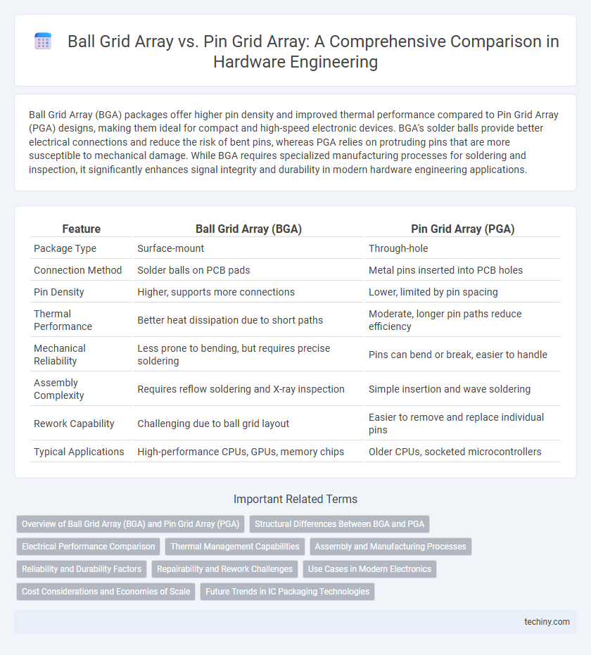
Table of Comparison
| Feature | Ball Grid Array (BGA) | Pin Grid Array (PGA) |
|---|---|---|
| Package Type | Surface-mount | Through-hole |
| Connection Method | Solder balls on PCB pads | Metal pins inserted into PCB holes |
| Pin Density | Higher, supports more connections | Lower, limited by pin spacing |
| Thermal Performance | Better heat dissipation due to short paths | Moderate, longer pin paths reduce efficiency |
| Mechanical Reliability | Less prone to bending, but requires precise soldering | Pins can bend or break, easier to handle |
| Assembly Complexity | Requires reflow soldering and X-ray inspection | Simple insertion and wave soldering |
| Rework Capability | Challenging due to ball grid layout | Easier to remove and replace individual pins |
| Typical Applications | High-performance CPUs, GPUs, memory chips | Older CPUs, socketed microcontrollers |
Overview of Ball Grid Array (BGA) and Pin Grid Array (PGA)
Ball Grid Array (BGA) packages feature an array of solder balls on the package bottom, offering improved thermal performance and efficient electrical connections for high-density integrated circuits. Pin Grid Array (PGA) packages use protruding pins arranged in a grid pattern on the underside, allowing easy socket insertion and replacement, commonly used in microprocessors. BGAs provide better mechanical stability and reduced signal inductance compared to PGAs, making them suitable for modern hardware engineering applications requiring compact, high-performance designs.
Structural Differences Between BGA and PGA
Ball Grid Array (BGA) packaging features an array of solder balls on the underside of the chip, enabling a lower profile and improved thermal performance compared to Pin Grid Array (PGA) which uses protruding pins arranged in a grid for socket insertion. BGA's solder balls provide uniform electrical connections with reduced inductance and resistance, enhancing signal integrity, whereas PGA pins are more susceptible to bending or damage during handling and insertion. The compact design of BGA allows for higher pin density and better heat dissipation, making it preferable in modern high-performance computing applications.
Electrical Performance Comparison
Ball Grid Array (BGA) packages exhibit superior electrical performance compared to Pin Grid Array (PGA) due to shorter interconnect lengths and reduced parasitic inductance and capacitance, which enhance signal integrity and allow higher frequency operation. BGA's solder balls provide more uniform electrical contact and lower resistance, minimizing signal loss and improving power distribution efficiency. In contrast, PGA designs suffer from longer lead lengths and increased susceptibility to noise and crosstalk, making them less optimal for high-speed applications.
Thermal Management Capabilities
Ball Grid Array (BGA) packages offer superior thermal management capabilities compared to Pin Grid Array (PGA) due to their direct solder ball connections that facilitate efficient heat dissipation through the PCB. BGA's lower thermal resistance and enhanced surface area contact enable better conduction of heat away from the chip, reducing thermal hotspots. In contrast, PGA designs rely on pins with limited contact area, resulting in higher thermal resistance and less effective heat transfer during high-performance or high-power applications.
Assembly and Manufacturing Processes
Ball Grid Array (BGA) packaging streamlines assembly with solder balls directly mounted on the chip underside, enabling automated placement and reflow soldering for higher connection density and reliability. Pin Grid Array (PGA) requires manual insertion of pins into sockets, increasing assembly complexity and potential for mechanical stress during installation and removal. BGA's use of stencil printing and precise reflow profiles significantly reduces manufacturing defects compared to PGA's more labor-intensive welding and socket alignment processes.
Reliability and Durability Factors
Ball Grid Array (BGA) packages exhibit superior reliability and durability compared to Pin Grid Array (PGA) due to their solder ball connections that offer better mechanical stability and lower thermal resistance. BGA's reduced susceptibility to pin damage and improved heat dissipation enhance long-term performance in high-stress environments. Conversely, PGA pins are prone to bending and mechanical failure, which can compromise electrical connections and overall device lifespan.
Repairability and Rework Challenges
Ball Grid Array (BGA) packages pose significant repairability and rework challenges due to their solder balls being hidden beneath the chip, making visual inspection and precise soldering difficult without specialized reflow equipment. In contrast, Pin Grid Array (PGA) packages offer easier access to individual pins, allowing straightforward manual repair and replacement, though they occupy more board space. The complexity of BGA rework often requires advanced X-ray inspection and hot air tools, increasing time and cost compared to the relatively simpler PGA processes.
Use Cases in Modern Electronics
Ball Grid Array (BGA) packages excel in high-density, high-performance applications like smartphones, gaming consoles, and networking equipment due to their superior thermal and electrical conductivity. Pin Grid Array (PGA) packages are favored for CPUs and microcontrollers requiring socketed connections, enabling easy replacement and upgrading in desktop computers and development environments. BGA is increasingly preferred in compact, high-speed devices where space and signal integrity are critical, whereas PGA remains relevant for prototyping and situations demanding mechanical robustness.
Cost Considerations and Economies of Scale
Ball Grid Array (BGA) packaging generally offers lower manufacturing costs at high volumes due to automated assembly processes and smaller package footprints, which reduce material usage and improve yield rates. Pin Grid Array (PGA) designs tend to incur higher costs because of manual socket assembly and larger package sizes that increase raw material expenses. Economies of scale favor BGA adoption in mass production, as its cost efficiency improves significantly with volume, whereas PGA remains cost-effective primarily in lower quantity or prototyping scenarios.
Future Trends in IC Packaging Technologies
Ball Grid Array (BGA) packaging continues to dominate due to its superior electrical performance, thermal management, and miniaturization capabilities compared to Pin Grid Array (PGA). Emerging trends emphasize advanced BGA variants like flip-chip BGA and embedded wafer-level ball grid array (eWLB) that enable higher input/output density and improved signal integrity for next-generation integrated circuits. Integration of heterogeneous materials and 3D stacking in BGA technology is driving the future of IC packaging, offering enhanced scalability and reliability in complex electronic systems.
Ball Grid Array vs Pin Grid Array Infographic