The chip package serves as the protective enclosure for the die, providing mechanical support and facilitating electrical connections between the die and the circuit board. While the die is the actual silicon semiconductor containing the integrated circuit, the package ensures durability, heat dissipation, and signal integrity in hardware engineering applications. Selecting the appropriate chip package is crucial for optimizing performance, cost, and reliability in electronic device manufacturing.
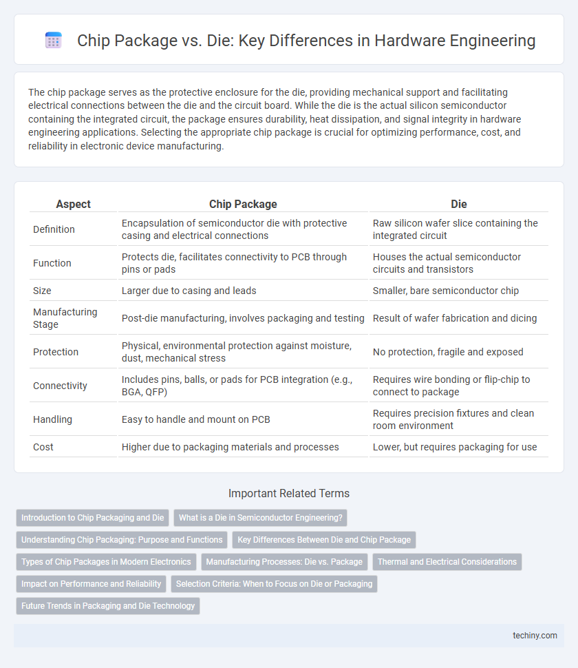
Table of Comparison
| Aspect | Chip Package | Die |
|---|---|---|
| Definition | Encapsulation of semiconductor die with protective casing and electrical connections | Raw silicon wafer slice containing the integrated circuit |
| Function | Protects die, facilitates connectivity to PCB through pins or pads | Houses the actual semiconductor circuits and transistors |
| Size | Larger due to casing and leads | Smaller, bare semiconductor chip |
| Manufacturing Stage | Post-die manufacturing, involves packaging and testing | Result of wafer fabrication and dicing |
| Protection | Physical, environmental protection against moisture, dust, mechanical stress | No protection, fragile and exposed |
| Connectivity | Includes pins, balls, or pads for PCB integration (e.g., BGA, QFP) | Requires wire bonding or flip-chip to connect to package |
| Handling | Easy to handle and mount on PCB | Requires precision fixtures and clean room environment |
| Cost | Higher due to packaging materials and processes | Lower, but requires packaging for use |
Introduction to Chip Packaging and Die
Chip packaging refers to the protective casing and interconnection system that houses the silicon die, ensuring mechanical support, thermal management, and electrical connectivity to the circuit board. The die is the bare semiconductor wafer slice containing the integrated circuit, responsible for the actual electronic functions within the chip. Understanding the relationship between the die and its package is crucial for optimizing performance, reliability, and manufacturability in hardware engineering.
What is a Die in Semiconductor Engineering?
A die in semiconductor engineering refers to the small block of silicon wafer that contains the integrated circuit components and is the fundamental building block of a chip package. It consists of transistors, resistors, and interconnects fabricated through photolithography and etching processes. The die is later encapsulated within a protective chip package that provides mechanical support, electrical connections, and thermal management for use in electronic devices.
Understanding Chip Packaging: Purpose and Functions
Chip packaging protects the die, the semiconductor material where circuits are etched, by encasing it in a durable enclosure that facilitates electrical connections and heat dissipation. The package serves as the interface between the die and the external environment, providing mechanical support, shielding against physical damage, and enabling reliable signal transmission to the printed circuit board. Understanding chip packaging is essential for optimizing performance, ensuring longevity, and supporting integration within electronic systems.
Key Differences Between Die and Chip Package
The die refers to the small, bare piece of semiconductor material where the integrated circuit is fabricated, while the chip package encompasses the die along with the protective casing and external connections. Key differences include the die being solely the silicon substrate with circuitry, whereas the chip package provides mechanical support, environmental protection, and facilitates electrical connection to the printed circuit board. The package significantly impacts heat dissipation, signal integrity, and overall reliability, making it a critical component in hardware engineering design.
Types of Chip Packages in Modern Electronics
Modern electronics utilize various types of chip packages, including Dual In-line Package (DIP), Quad Flat Package (QFP), Ball Grid Array (BGA), and Chip Scale Package (CSP). Each package type offers different benefits in terms of size, thermal management, and electrical performance, with BGA providing superior heat dissipation and improved signal integrity for high-density applications. The choice between chip package types depends on factors such as device complexity, application requirements, and manufacturing processes.
Manufacturing Processes: Die vs. Package
Die manufacturing involves photolithography, doping, etching, and metallization within semiconductor fabs to define transistor structures on silicon wafers. Package manufacturing includes substrate preparation, wire bonding or flip-chip attachment, molding, and final testing to protect the die and enable electrical connections. Die processes prioritize miniaturization and transistor performance, while package processes focus on mechanical protection, heat dissipation, and signal integrity.
Thermal and Electrical Considerations
Chip package design significantly impacts thermal dissipation and electrical performance, as it facilitates heat transfer from the die to the external environment and reduces electrical resistance. Die size, material composition, and interconnect topology directly influence thermal conductivity and signal integrity within the chip, necessitating optimized package materials like copper or ceramics. Proper thermal management in the package prevents overheating and ensures stable electrical connections, enhancing overall device reliability and performance.
Impact on Performance and Reliability
Chip package design significantly influences thermal management and signal integrity, directly affecting overall chip performance and reliability. Die quality determines core processing capabilities, but inadequate packaging can cause bottlenecks such as increased electrical resistance and heat dissipation issues. Optimizing both chip package and die integration ensures enhanced speed, reduced failure rates, and prolonged device lifespan.
Selection Criteria: When to Focus on Die or Packaging
Die selection emphasizes intrinsic semiconductor performance metrics such as transistor count, die size, power consumption, and thermal conductivity, making it crucial for high-speed processors and advanced integrated circuits. Packaging selection focuses on mechanical protection, signal integrity, heat dissipation, and interface requirements, which are critical for applications requiring robust environmental resistance and system-level integration. Designers prioritize die when optimizing raw electrical performance, whereas packaging becomes the focal point for enhancing reliability, manufacturability, and end-product compliance.
Future Trends in Packaging and Die Technology
Advancements in chip package and die technology are driving the future of hardware engineering, with trends emphasizing 3D integration, heterogeneous packaging, and advanced materials that enhance performance and thermal management. Die stacking and chiplet architectures are enabling higher density and modular designs, reducing latency and improving scalability. Emerging solutions like wafer-level packaging and embedded dies are set to revolutionize system miniaturization and power efficiency in next-generation semiconductor devices.
Chip Package vs Die Infographic