Dual-layer PCBs offer two conductive layers which provide increased circuit density and improved routing compared to single-layer boards, making them suitable for moderately complex hardware designs. Multi-layer PCBs incorporate three or more layers, enabling higher component integration, enhanced signal integrity, and reduced electromagnetic interference in advanced electronic systems. Choosing between dual-layer and multi-layer PCBs depends on the complexity, size constraints, and electrical performance requirements of the hardware project.
Table of Comparison
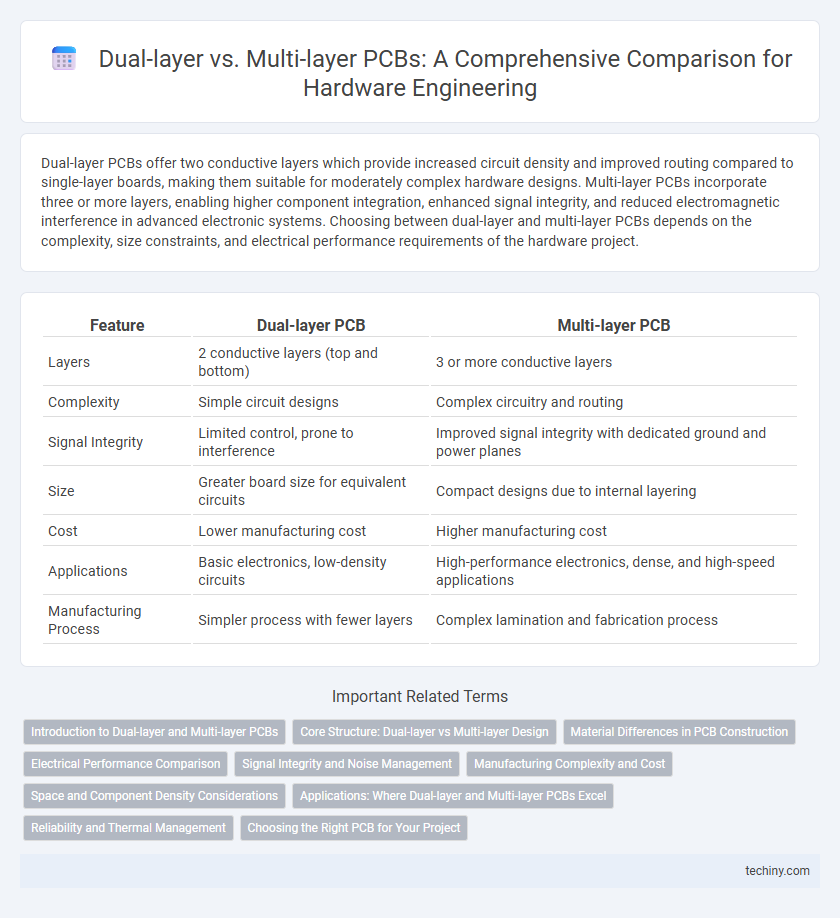
| Feature | Dual-layer PCB | Multi-layer PCB |
|---|---|---|
| Layers | 2 conductive layers (top and bottom) | 3 or more conductive layers |
| Complexity | Simple circuit designs | Complex circuitry and routing |
| Signal Integrity | Limited control, prone to interference | Improved signal integrity with dedicated ground and power planes |
| Size | Greater board size for equivalent circuits | Compact designs due to internal layering |
| Cost | Lower manufacturing cost | Higher manufacturing cost |
| Applications | Basic electronics, low-density circuits | High-performance electronics, dense, and high-speed applications |
| Manufacturing Process | Simpler process with fewer layers | Complex lamination and fabrication process |
Introduction to Dual-layer and Multi-layer PCBs
Dual-layer PCBs consist of two conductive copper layers separated by an insulating substrate, enabling simple circuit designs with moderate component density. Multi-layer PCBs incorporate three or more copper layers stacked together, allowing for complex circuitry, enhanced signal integrity, and reduced electromagnetic interference. These multi-layer boards are essential for advanced hardware engineering applications requiring compact, high-performance designs.
Core Structure: Dual-layer vs Multi-layer Design
Dual-layer PCBs consist of two conductive copper layers separated by an insulating substrate, enabling simple routing and higher density than single-layer boards. Multi-layer PCBs integrate three or more layers with alternating core and prepreg materials, allowing complex circuit designs and enhanced signal integrity through dedicated power and ground planes. The core structure difference impacts manufacturing complexity, electrical performance, and overall board thickness, making multi-layer PCBs suitable for advanced hardware engineering applications requiring compact, high-speed circuits.
Material Differences in PCB Construction
Dual-layer PCBs typically consist of two copper layers separated by an insulating substrate like FR-4, offering moderate complexity and flexibility for simpler circuit designs. Multi-layer PCBs feature three or more copper layers laminated with alternating insulating layers, often using advanced materials such as high-Tg FR-4 or polyimide to enhance thermal stability and electrical performance. The choice of materials in multi-layer PCBs supports higher signal integrity and durability, making them suitable for complex, high-density hardware engineering applications.
Electrical Performance Comparison
Dual-layer PCBs provide improved signal integrity compared to single-layer designs by offering a dedicated ground plane, which reduces electromagnetic interference and crosstalk. Multi-layer PCBs further enhance electrical performance through multiple signal and ground layers, enabling shorter signal paths, controlled impedance, and superior noise isolation. The increased layer count in multi-layer PCBs supports higher frequency applications and complex circuitry with better power distribution and reduced signal attenuation.
Signal Integrity and Noise Management
Dual-layer PCBs offer improved signal integrity over single-layer boards by providing dedicated ground planes that reduce electromagnetic interference (EMI), but they have limitations in handling complex high-speed signals compared to multi-layer PCBs. Multi-layer PCBs, with multiple dedicated signal and ground planes, enhance noise management by minimizing crosstalk and ensuring controlled impedance, critical for high-frequency circuits and advanced hardware engineering applications. Effective stack-up design in multi-layer PCBs significantly reduces signal distortion and power distribution issues, optimizing performance in modern electronic systems.
Manufacturing Complexity and Cost
Dual-layer PCBs have moderate manufacturing complexity with two conductive layers and limited via requirements, resulting in lower production costs compared to multi-layer PCBs. Multi-layer PCBs involve complex fabrication processes due to multiple stacked layers and intricate via interconnections, significantly increasing manufacturing time and expenses. The enhanced signal integrity and design density of multi-layer PCBs justify the higher cost in high-performance hardware engineering applications.
Space and Component Density Considerations
Dual-layer PCBs offer moderate space efficiency with components placed on both sides, enabling limited routing complexity suitable for simpler hardware designs. Multi-layer PCBs significantly enhance space utilization by stacking multiple conductive layers, allowing higher component density and complex interconnections required in advanced hardware engineering. The increased layer count in multi-layer PCBs optimizes board real estate, reduces electromagnetic interference, and supports miniaturization in compact electronic devices.
Applications: Where Dual-layer and Multi-layer PCBs Excel
Dual-layer PCBs excel in automotive electronics, consumer gadgets, and basic industrial controls where moderate circuit complexity and cost-efficiency are critical. Multi-layer PCBs dominate high-performance computing, telecommunications, and aerospace systems requiring dense component integration, superior signal integrity, and advanced thermal management. Applications such as medical imaging and advanced robotics benefit from multi-layer designs due to their ability to support complex, high-speed signal routing and power distribution.
Reliability and Thermal Management
Dual-layer PCBs offer improved reliability due to simpler construction and fewer interlayer connections that reduce failure points, making them suitable for less complex hardware designs. Multi-layer PCBs enhance thermal management by incorporating additional internal copper layers that dissipate heat more efficiently, which is critical for high-performance and densely packed electronic components. The increased complexity and number of layers in multi-layer PCBs can introduce potential reliability challenges, but advanced manufacturing techniques and materials help mitigate thermal stress and maintain circuit integrity.
Choosing the Right PCB for Your Project
Choosing the right PCB for your hardware engineering project depends on factors such as signal integrity, complexity, and cost. Dual-layer PCBs offer improved routing and reduced electromagnetic interference compared to single-layer designs, making them suitable for moderately complex circuits. Multi-layer PCBs provide enhanced performance for high-density and high-speed applications by enabling more compact routing, superior power distribution, and better thermal management.
Dual-layer vs Multi-layer PCB Infographic