A four-layer PCB offers improved signal integrity and better electromagnetic interference (EMI) shielding compared to a two-layer PCB, making it ideal for complex hardware engineering projects requiring high-speed signal processing. The additional layers in a four-layer PCB enable dedicated power and ground planes, reducing noise and enhancing overall circuit performance. While two-layer PCBs are cost-effective and suitable for simpler designs, four-layer PCBs provide enhanced reliability and design flexibility for advanced electronic applications.
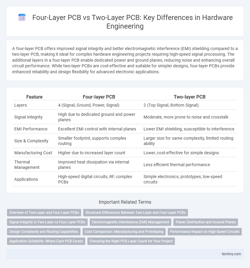
Table of Comparison
| Feature | Four-layer PCB | Two-layer PCB |
|---|---|---|
| Layers | 4 (Signal, Ground, Power, Signal) | 2 (Top Signal, Bottom Signal) |
| Signal Integrity | High due to dedicated ground and power planes | Moderate, more prone to noise and crosstalk |
| EMI Performance | Excellent EMI control with internal planes | Lower EMI shielding, susceptible to interference |
| Size & Complexity | Smaller footprint, supports complex routing | Larger size for same complexity, limited routing ability |
| Manufacturing Cost | Higher due to increased layer count | Lower, cost-effective for simple designs |
| Thermal Management | Improved heat dissipation via internal planes | Less efficient thermal performance |
| Applications | High-speed digital circuits, RF, complex PCBs | Simple electronics, prototypes, low-speed circuits |
Overview of Two-Layer and Four-Layer PCBs
Two-layer PCBs consist of two conductive copper layers separated by an insulating substrate, enabling basic circuit designs with limited complexity and signal integrity. Four-layer PCBs include two additional internal layers, typically used for power and ground planes, enhancing electromagnetic compatibility and supporting higher-speed circuits. The increased layering in four-layer PCBs improves thermal management, reduces noise, and allows for more compact and reliable hardware engineering solutions.
Structural Differences Between Two-Layer and Four-Layer PCBs
Two-layer PCBs consist of two conductive copper layers separated by an insulating substrate, offering basic routing capabilities suitable for simple circuits. Four-layer PCBs feature an additional pair of internal layers, usually dedicated to power and ground planes, which enhance signal integrity, reduce electromagnetic interference, and improve thermal management. The structural complexity of four-layer PCBs supports higher component density and more reliable electrical performance compared to two-layer designs.
Signal Integrity in Two-Layer vs Four-Layer PCBs
Four-layer PCBs significantly improve signal integrity compared to two-layer PCBs by providing dedicated ground and power planes that reduce electromagnetic interference and crosstalk. The controlled impedance and reduced loop inductance in four-layer designs facilitate stable high-speed signal transmission, essential for complex hardware engineering applications. Two-layer PCBs often suffer from increased signal noise and degraded performance due to limited layer stacking and less effective signal return paths.
Electromagnetic Interference (EMI) Management
Four-layer PCBs offer superior electromagnetic interference (EMI) management due to their dedicated ground and power planes, which significantly reduce noise and signal crosstalk compared to two-layer PCBs. The additional layers provide better signal integrity by minimizing loop areas and allowing controlled impedance traces, effectively dissipating EMI emissions. Design practitioners prefer four-layer PCBs in high-frequency applications where stringent EMI standards are required to ensure system reliability and electromagnetic compatibility (EMC).
Power Distribution and Ground Planes
Four-layer PCBs offer superior power distribution and ground plane management compared to two-layer PCBs, featuring dedicated internal layers for power and ground that reduce electromagnetic interference and signal crosstalk. The separated planes enhance signal integrity by providing low-impedance return paths and minimizing voltage fluctuations across the board. Two-layer PCBs lack dedicated planes, often resulting in compromised power stability and increased noise levels, making four-layer designs preferable for complex hardware engineering applications requiring reliable power delivery and signal quality.
Design Complexity and Routing Capabilities
Four-layer PCBs offer enhanced design complexity and superior routing capabilities compared to two-layer PCBs due to additional signal and power planes, which facilitate better electromagnetic interference (EMI) control and reduced crosstalk. The extra layers enable more intricate circuit designs, allowing for higher component density and simplified routing paths, crucial for high-speed and high-frequency applications. Two-layer PCBs often face limitations in trace routing and signal integrity, making them less suitable for complex hardware engineering projects that demand optimized performance and reliability.
Cost Comparison: Manufacturing and Prototyping
Four-layer PCBs incur higher manufacturing costs compared to two-layer PCBs due to increased material usage, complexity in lamination processes, and longer production times. Prototyping expenses also rise with four-layer boards as advanced equipment and more precise quality control measures are required to ensure signal integrity and layer alignment. Despite the cost differential, four-layer PCBs offer improved electrical performance and noise reduction, which can be critical for complex hardware engineering applications.
Performance Impact on High-Speed Circuits
Four-layer PCBs offer significantly improved signal integrity and reduced electromagnetic interference compared to two-layer PCBs, crucial for high-speed circuit performance. The additional layers enable dedicated power and ground planes, minimizing crosstalk and signal distortion. This layered structure enhances impedance control and thermal management, resulting in faster, more reliable signal transmission in complex hardware designs.
Application Suitability: Where Each PCB Excels
Four-layer PCBs excel in complex, high-speed applications such as aerospace, telecommunications, and advanced computing due to their superior signal integrity and reduced electromagnetic interference. Two-layer PCBs are ideally suited for simpler, cost-sensitive projects like consumer electronics and basic industrial devices where design complexity and electromagnetic control are less critical. Choosing between four-layer and two-layer PCBs depends on the specific requirements for thermal management, noise reduction, and circuit density in the intended hardware application.
Choosing the Right PCB Layer Count for Your Project
Selecting the appropriate PCB layer count depends on factors such as signal integrity, space constraints, and electromagnetic interference management. Four-layer PCBs provide superior power distribution and grounding planes, reducing noise and improving high-frequency performance compared to two-layer PCBs. For complex designs with dense routing or mixed-signal applications, four-layer boards enhance reliability and simplify layout, while two-layer PCBs remain cost-effective for simpler, low-density circuits.
Four-layer PCB vs Two-layer PCB Infographic