Multilayer PCBs offer greater circuit density and improved electrical performance compared to single-layer PCBs, making them ideal for complex hardware designs. They support multiple signal layers, power planes, and ground planes, which reduce electromagnetic interference and enhance signal integrity. Single-layer PCBs, while simpler and more cost-effective, are best suited for basic electronic applications with limited routing requirements.
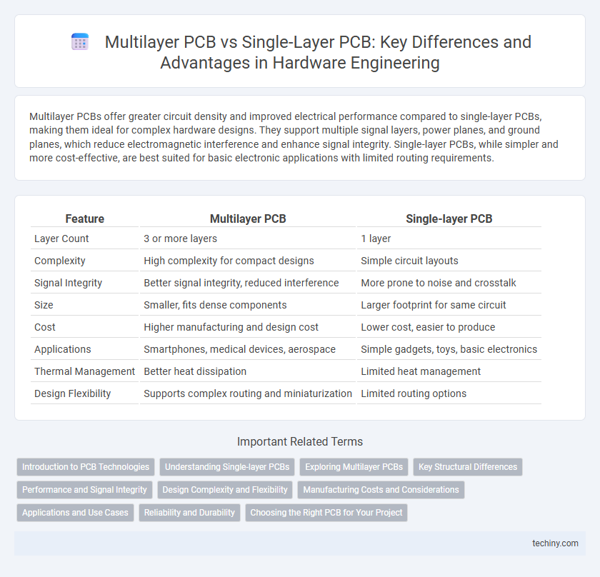
Table of Comparison
| Feature | Multilayer PCB | Single-layer PCB |
|---|---|---|
| Layer Count | 3 or more layers | 1 layer |
| Complexity | High complexity for compact designs | Simple circuit layouts |
| Signal Integrity | Better signal integrity, reduced interference | More prone to noise and crosstalk |
| Size | Smaller, fits dense components | Larger footprint for same circuit |
| Cost | Higher manufacturing and design cost | Lower cost, easier to produce |
| Applications | Smartphones, medical devices, aerospace | Simple gadgets, toys, basic electronics |
| Thermal Management | Better heat dissipation | Limited heat management |
| Design Flexibility | Supports complex routing and miniaturization | Limited routing options |
Introduction to PCB Technologies
Multilayer PCBs consist of three or more conductive layers stacked together, enabling complex circuitry and higher component density compared to single-layer PCBs, which have only one conductive layer on a single substrate. Multilayer designs provide enhanced electrical performance, signal integrity, and reduced electromagnetic interference, making them ideal for advanced hardware applications in telecommunications, aerospace, and computing devices. Single-layer PCBs are simpler and cost-effective, suitable for basic electronic devices with minimal circuitry requirements.
Understanding Single-layer PCBs
Single-layer PCBs consist of a single substrate layer with one conductive copper layer used for circuit routing, making them simpler and cost-effective for basic electronic devices. These PCBs support fewer components and connections, which limits complex circuit designs but offers ease of manufacturing and repair. Their reliability in low-density applications makes them a preferred choice for consumer electronics, lighting, and power supplies.
Exploring Multilayer PCBs
Multilayer PCBs consist of multiple layers of conductive traces separated by insulating materials, enabling complex circuit designs and higher component density compared to single-layer PCBs. They support improved electrical performance, reduced electromagnetic interference, and enhanced signal integrity, making them ideal for advanced hardware engineering applications. Multilayer PCBs also facilitate miniaturization of devices and increased functionality within compact spaces.
Key Structural Differences
Multilayer PCBs consist of three or more conductive layers separated by insulating material, enabling higher circuit density and more complex designs compared to single-layer PCBs, which contain only one conductive layer. The multilayer structure enhances signal integrity and electromagnetic compatibility by incorporating ground and power planes, whereas single-layer PCBs typically experience more electromagnetic interference. Thermal management is also improved in multilayer PCBs due to additional layers that facilitate heat dissipation, making them suitable for advanced hardware engineering applications.
Performance and Signal Integrity
Multilayer PCBs offer superior performance and enhanced signal integrity compared to single-layer PCBs due to their multiple conductive layers, which reduce electromagnetic interference and provide better impedance control. Advanced dielectric materials used in multilayer PCBs minimize signal loss and crosstalk, ensuring high-frequency signal fidelity essential for complex hardware systems. Single-layer PCBs, limited by their single conductive path, typically exhibit higher noise susceptibility and less efficient power distribution, making them less suitable for high-speed or high-density applications.
Design Complexity and Flexibility
Multilayer PCBs offer significantly higher design complexity and flexibility compared to single-layer PCBs by allowing multiple signal layers, power planes, and ground planes to be integrated within a compact footprint. This multilayer structure enables advanced circuit routing and improved electromagnetic interference (EMI) control, essential for high-speed and high-density applications. Single-layer PCBs, while simpler and less costly, are limited in routing options and cannot support complex or high-performance designs.
Manufacturing Costs and Considerations
Multilayer PCBs generally incur higher manufacturing costs due to the complex fabrication processes involving multiple layers of copper and insulating materials, increased drilling precision, and stringent quality control measures. Single-layer PCBs are more cost-effective, given their simpler design and faster production times, making them ideal for low-budget or less complex applications. Manufacturing considerations for multilayer PCBs include potential issues such as layer misalignment and thermal management, which can increase both production time and expenses.
Applications and Use Cases
Multilayer PCBs are essential in complex hardware engineering applications requiring high-density circuits, such as smartphones, aerospace electronics, and medical devices, due to their compact design and enhanced signal integrity. Single-layer PCBs suit simpler, cost-sensitive products like household appliances, LED lighting, and basic instrumentation where minimal circuitry suffices. Multilayer boards enable advanced functionality and miniaturization, while single-layer options provide straightforward, budget-friendly solutions for less demanding electronic components.
Reliability and Durability
Multilayer PCBs offer enhanced reliability and durability compared to single-layer PCBs due to their multiple conductive layers that improve signal integrity and reduce electromagnetic interference. The compact structure of multilayer PCBs ensures robust performance in harsh environments, making them ideal for complex and high-frequency applications. Single-layer PCBs, while simpler and cost-effective, are more prone to damage and signal loss, limiting their lifespan and reliability in demanding hardware engineering projects.
Choosing the Right PCB for Your Project
Selecting the right PCB for your hardware engineering project hinges on factors such as complexity, space constraints, and signal integrity requirements. Multilayer PCBs offer enhanced performance with multiple signal layers ideal for high-density and high-speed applications, while single-layer PCBs provide simplicity and cost-effectiveness for straightforward circuits. Evaluating project specifications, including electrical and mechanical demands, ensures optimal PCB choice for reliability and functionality.
Multilayer PCB vs Single-layer PCB Infographic