Open Collector and Open Drain outputs are both types of transistor configurations used for digital signals, allowing multiple devices to share a line without damage. Open Collector refers specifically to bipolar transistor outputs, whereas Open Drain applies to MOSFET transistor outputs. Both configurations require an external pull-up resistor to achieve proper signal levels and are commonly used in wired-AND or wired-OR logic circuits for hardware engineering applications.
Table of Comparison
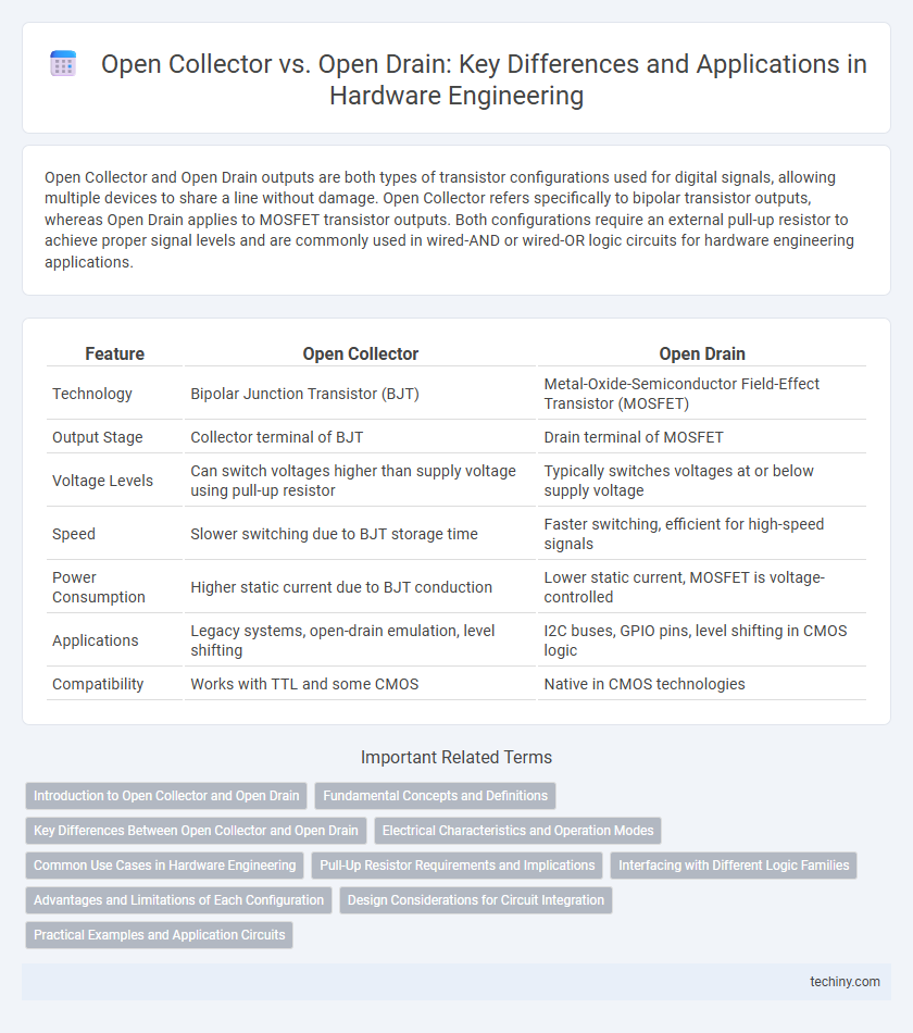
| Feature | Open Collector | Open Drain |
|---|---|---|
| Technology | Bipolar Junction Transistor (BJT) | Metal-Oxide-Semiconductor Field-Effect Transistor (MOSFET) |
| Output Stage | Collector terminal of BJT | Drain terminal of MOSFET |
| Voltage Levels | Can switch voltages higher than supply voltage using pull-up resistor | Typically switches voltages at or below supply voltage |
| Speed | Slower switching due to BJT storage time | Faster switching, efficient for high-speed signals |
| Power Consumption | Higher static current due to BJT conduction | Lower static current, MOSFET is voltage-controlled |
| Applications | Legacy systems, open-drain emulation, level shifting | I2C buses, GPIO pins, level shifting in CMOS logic |
| Compatibility | Works with TTL and some CMOS | Native in CMOS technologies |
Introduction to Open Collector and Open Drain
Open Collector and Open Drain configurations both function as transistor outputs that can only sink current, requiring an external pull-up resistor to achieve a defined high level. Open Collector uses bipolar junction transistors (BJTs), while Open Drain relies on metal-oxide-semiconductor field-effect transistors (MOSFETs), affecting voltage levels and switching characteristics. These configurations enable wired-AND logic and are commonly found in communication buses and interrupt lines within hardware engineering.
Fundamental Concepts and Definitions
Open collector and open drain are both transistor output configurations used in digital circuits to allow multiple devices to share a common bus without damage. An open collector uses bipolar junction transistor (BJT) technology where the collector is left unconnected internally, relying on an external pull-up resistor to define the high level. Open drain refers to the MOSFET equivalent, where the drain terminal is left open and requires an external pull-up resistor, enabling wired-AND logic and facilitating signal level translation in hardware engineering applications.
Key Differences Between Open Collector and Open Drain
Open collector and open drain configurations both function as transistor outputs used for wired-AND logic but differ in semiconductor type and voltage compatibility; open collector uses bipolar junction transistors (BJTs) and is typically found in 5V TTL systems, while open drain employs MOSFETs and is compatible with a wider range of voltage levels in CMOS technology. Open collector outputs require an external pull-up resistor tied to the supply voltage to drive the line high, whereas open drain outputs also need a pull-up resistor but benefit from lower power consumption and faster switching speeds due to MOSFET characteristics. Understanding these distinctions aids in selecting the appropriate interface for mixed-signal circuits and ensures optimal integration with microcontrollers and sensor networks.
Electrical Characteristics and Operation Modes
Open collector and open drain configurations both operate by allowing the output transistor to sink current while requiring an external pull-up resistor to achieve a high logic level. Open collector circuits use bipolar junction transistors (BJTs) with the collector terminal left unconnected internally, suitable for higher voltage levels typically in TTL logic families. Open drain circuits employ MOSFET transistors with the drain terminal exposed externally, optimized for lower voltage operations in CMOS environments, offering faster switching speeds and lower power consumption.
Common Use Cases in Hardware Engineering
Open collector and open drain configurations are widely used in hardware engineering for interfacing multiple outputs to a single bus or line, enabling wired-AND logic and simplifying inter-device communication. Open collector circuits are primarily found in TTL logic systems, while open drain configurations are employed in CMOS devices, both allowing for level shifting and bus sharing. Common applications include I2C bus communication, interrupt lines, and driving LEDs or relays where multiple signals must be combined without direct output conflicts.
Pull-Up Resistor Requirements and Implications
Open Collector and Open Drain configurations both require pull-up resistors to maintain a defined high logic level when the transistor is not conducting; this resistor plays a crucial role in determining the signal rise time and noise immunity. In Open Collector circuits, which use bipolar junction transistors (BJTs), the pull-up resistor must be carefully selected to balance current consumption and switching speed, typically ranging from 1 kO to 10 kO, while Open Drain circuits with MOSFETs exhibit lower leakage current, allowing for higher-value pull-ups and lower power dissipation. Improper sizing of the pull-up resistor in either configuration can lead to increased power loss, slower edge transitions, and potential signal integrity issues, impacting overall hardware performance and reliability.
Interfacing with Different Logic Families
Open collector and open drain outputs enable interfacing between different logic families by allowing multiple devices to share a common bus line through a wired-AND connection. Open collector, typically used in bipolar transistor circuits, and open drain, found in MOSFET devices, both require pull-up resistors to establish the high-level voltage compatible with various logic standards. This flexibility ensures proper voltage level translation and signal integrity when integrating TTL, CMOS, or other logic families in mixed-signal systems.
Advantages and Limitations of Each Configuration
Open collector outputs allow multiple outputs to be wired together safely for wired-AND logic functions, offering flexibility in mixed-voltage systems, but require an external pull-up resistor which can slow signal transitions. Open drain configurations, used primarily in MOSFET technologies, provide similar wired-AND capabilities with lower power consumption and higher speed due to the inherent transistor structure but also need pull-up resistors to define the logic high level. Both configurations face limitations in speed and noise immunity compared to push-pull outputs, with open collector circuits being more common in bipolar designs and open drain favored in CMOS-based systems.
Design Considerations for Circuit Integration
Open collector and open drain outputs require pull-up resistors for proper signal levels, with open collector typically used in bipolar transistor circuits and open drain in MOSFET designs. Design considerations include voltage tolerance, switching speed, and logic level compatibility to ensure reliable integration within mixed-technology systems. Careful selection of pull-up resistors and evaluation of current sinking capabilities are critical for minimizing power consumption and preventing signal integrity issues in complex hardware engineering projects.
Practical Examples and Application Circuits
Open Collector outputs are commonly used with bipolar transistors in interfacing TTL logic levels, allowing multiple outputs to wire-OR by connecting their collectors to a shared pull-up resistor. Open Drain configurations, typical in MOSFET-based circuits like I2C buses, use the transistor's drain terminal to pull the line low, enabling bidirectional communication with external pull-up resistors. Practical application circuits include microcontroller GPIO pins configured as open drain for driving LEDs or level shifting, while open collector outputs are frequently employed in relay driving and wired-AND logic implementations.
Open Collector vs Open Drain Infographic