Parasitic capacitance and parasitic inductance are critical factors influencing hardware engineering performance, where parasitic capacitance arises from unintended electric fields between conductive elements causing signal delay and crosstalk. Parasitic inductance, caused by loop areas and conductor geometry, induces unwanted voltage spikes and signal integrity issues at high frequencies. Optimizing PCB layouts and component placement mitigates these parasitic effects, enhancing overall circuit reliability and speed.
Table of Comparison
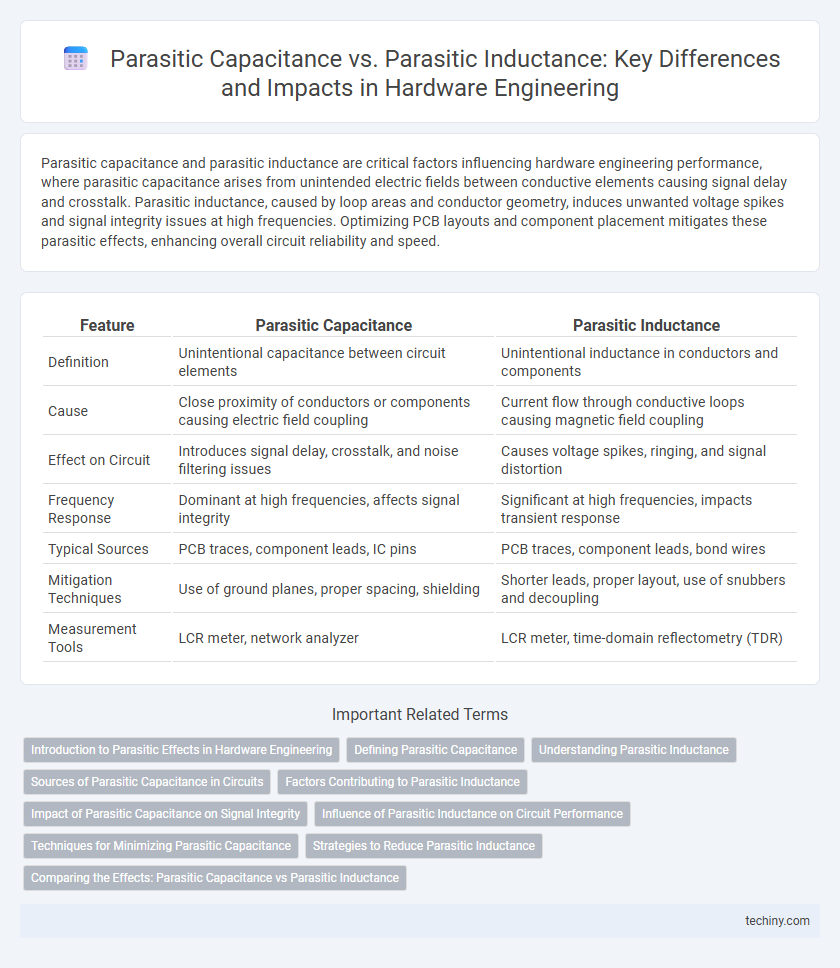
| Feature | Parasitic Capacitance | Parasitic Inductance |
|---|---|---|
| Definition | Unintentional capacitance between circuit elements | Unintentional inductance in conductors and components |
| Cause | Close proximity of conductors or components causing electric field coupling | Current flow through conductive loops causing magnetic field coupling |
| Effect on Circuit | Introduces signal delay, crosstalk, and noise filtering issues | Causes voltage spikes, ringing, and signal distortion |
| Frequency Response | Dominant at high frequencies, affects signal integrity | Significant at high frequencies, impacts transient response |
| Typical Sources | PCB traces, component leads, IC pins | PCB traces, component leads, bond wires |
| Mitigation Techniques | Use of ground planes, proper spacing, shielding | Shorter leads, proper layout, use of snubbers and decoupling |
| Measurement Tools | LCR meter, network analyzer | LCR meter, time-domain reflectometry (TDR) |
Introduction to Parasitic Effects in Hardware Engineering
Parasitic capacitance and parasitic inductance are unintended electrical properties that arise from the physical layout and materials of hardware components, significantly affecting circuit performance. Parasitic capacitance occurs due to the close proximity of conductive elements storing electric charge, leading to unwanted coupling and signal distortion. Parasitic inductance results from the inherent inductance of conductive paths, causing voltage spikes and signal integrity issues in high-frequency circuits.
Defining Parasitic Capacitance
Parasitic capacitance refers to the unintended and undesirable capacitance that occurs between conductive elements in electronic circuits, such as between adjacent wires or components. This phenomenon can cause signal distortion, crosstalk, and reduced circuit performance by storing and releasing electrical energy within the circuit. Understanding parasitic capacitance is critical for hardware engineers to optimize high-frequency circuit designs and minimize signal integrity issues.
Understanding Parasitic Inductance
Parasitic inductance arises from the inherent inductive properties of conductive paths, such as PCB traces and component leads, causing unwanted voltage spikes and signal integrity issues at high frequencies. It is critical to minimize parasitic inductance in hardware engineering by optimizing trace geometry, using shorter leads, and implementing ground planes to reduce loop areas. Understanding the impact of parasitic inductance enables engineers to improve high-speed circuit performance and mitigate electromagnetic interference (EMI).
Sources of Parasitic Capacitance in Circuits
Parasitic capacitance in hardware circuits primarily originates from the close proximity of conductive elements, such as overlapping metal layers, component leads, and PCB traces separated by dielectric materials. Key sources include inter-layer coupling in multi-layer PCBs, junctions in semiconductor devices, and the parasitic effects of packaging and connectors. Understanding and minimizing these capacitances is crucial for high-frequency circuit performance and signal integrity.
Factors Contributing to Parasitic Inductance
Parasitic inductance in hardware engineering arises primarily from the physical geometry of conductors, including trace length, width, and loop area, which collectively increase the magnetic field interaction. The choice of materials, such as the substrate and conductor type, also influences inductance due to varying magnetic permeability and conductivity. High-frequency operation further accentuates these effects by increasing the influence of skin effect and mutual inductance between adjacent circuit elements.
Impact of Parasitic Capacitance on Signal Integrity
Parasitic capacitance significantly affects signal integrity by causing unintended coupling between circuit nodes, leading to signal distortion and timing errors in high-speed digital circuits. This unwanted capacitance introduces delays and attenuates signal edges, resulting in reduced signal bandwidth and increased cross-talk in densely packed PCB layouts. Minimizing parasitic capacitance through careful PCB design and component placement is crucial for maintaining signal integrity and overall circuit performance in hardware engineering.
Influence of Parasitic Inductance on Circuit Performance
Parasitic inductance in hardware engineering significantly affects circuit performance by causing unwanted voltage spikes and signal integrity issues, particularly in high-frequency applications. This inductance can lead to slower switching speeds and increased electromagnetic interference (EMI), degrading overall system reliability. Minimizing parasitic inductance through careful PCB layout and component selection is crucial for maintaining optimal circuit functionality and reducing noise.
Techniques for Minimizing Parasitic Capacitance
Minimizing parasitic capacitance in hardware engineering involves careful layout design, such as increasing the spacing between conductive traces and using low-k dielectric materials to reduce the capacitance between components. Shielding techniques and the implementation of ground planes can effectively isolate sensitive nodes, thereby lowering unwanted capacitive coupling. Employing multi-layer PCB designs and optimizing component placement further decreases parasitic effects, enhancing signal integrity and overall circuit performance.
Strategies to Reduce Parasitic Inductance
Minimizing parasitic inductance in hardware engineering involves shortening and widening PCB traces to reduce inductive loops, using ground planes to provide low-inductance return paths, and placing decoupling capacitors close to integrated circuits to suppress high-frequency noise. Implementing multiple vias in parallel decreases inductance by improving current distribution, while using low-inductance component packaging and carefully routing power and signal lines further limits unwanted inductive effects. Optimizing layer stack-up and maintaining symmetrical layouts also help reduce parasitic inductance in high-speed circuits.
Comparing the Effects: Parasitic Capacitance vs Parasitic Inductance
Parasitic capacitance causes unwanted coupling between circuit elements, leading to signal distortion and reduced high-frequency performance, while parasitic inductance results in voltage spikes and ringing due to sudden current changes in conductors. The impact of parasitic capacitance is prominent in high-speed digital circuits where it degrades signal integrity, whereas parasitic inductance primarily affects power delivery networks and switching devices by inducing electromagnetic interference (EMI). Effective hardware engineering addresses both by optimizing PCB layout, using proper component placement, and employing techniques such as ground planes and decoupling capacitors to mitigate these parasitic effects.
Parasitic Capacitance vs Parasitic Inductance Infographic