Phase-Locked Loops (PLLs) are widely used in hardware engineering for frequency synthesis and clock generation, offering precise control over output frequency by locking to a reference signal. Delay-Locked Loops (DLLs) provide fine timing adjustments by aligning the phase of the output clock with the reference clock, minimizing clock skew in integrated circuits. While PLLs excel in generating stable frequencies, DLLs are preferred for phase alignment tasks in high-speed digital applications.
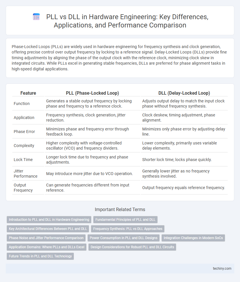
Table of Comparison
| Feature | PLL (Phase-Locked Loop) | DLL (Delay-Locked Loop) |
|---|---|---|
| Function | Generates a stable output frequency by locking phase and frequency to a reference clock. | Adjusts output delay to match the input clock phase without frequency synthesis. |
| Application | Frequency synthesis, clock generation, jitter reduction. | Clock deskew, timing adjustment, phase alignment. |
| Phase Error | Minimizes phase and frequency error through feedback loop. | Minimizes only phase error by adjusting delay line. |
| Complexity | Higher complexity with voltage-controlled oscillator (VCO) and frequency dividers. | Lower complexity, primarily uses variable delay elements. |
| Lock Time | Longer lock time due to frequency and phase adjustments. | Shorter lock time; locks phase quickly. |
| Jitter Performance | May introduce more jitter due to VCO operation. | Generally lower jitter as no frequency synthesis involved. |
| Output Frequency | Can generate frequencies different from input reference. | Output frequency equals reference frequency. |
Introduction to PLL and DLL in Hardware Engineering
Phase-Locked Loop (PLL) and Delay-Locked Loop (DLL) are essential components in hardware engineering used for clock synchronization and timing adjustments within integrated circuits. PLL continuously adjusts the phase of a voltage-controlled oscillator to match the phase of a reference signal, enabling frequency multiplication and jitter reduction. DLL uses a series of delay elements to align the clock output phase directly with the input reference, providing fine timing control with lower jitter and faster lock times compared to PLLs.
Fundamental Principles of PLL and DLL
Phase-Locked Loop (PLL) operates by continuously adjusting the phase of a voltage-controlled oscillator (VCO) to match the phase of a reference signal, effectively minimizing phase difference through a feedback control system. Delay-Locked Loop (DLL) aligns the timing of an output clock signal by continuously delaying the reference clock in increments until the phases coincide, relying on a variable delay line rather than an oscillator. The fundamental distinction lies in PLL's use of frequency adjustment via VCO for phase alignment, whereas DLL achieves alignment solely through controlled delay without generating a new frequency.
Key Architectural Differences Between PLL and DLL
Phase-Locked Loops (PLL) use a voltage-controlled oscillator and a feedback loop to synchronize the output phase and frequency with the input reference, while Delay-Locked Loops (DLL) rely on a variable delay line to adjust the timing of the output signal. PLLs generate a new clock signal with frequency multiplication capabilities, whereas DLLs primarily provide phase alignment without frequency alteration. The inherent frequency synthesis feature of PLLs contrasts with DLLs' focus on minimizing clock skew and jitter through phase delay adjustments.
Frequency Synthesis: PLL vs DLL Approaches
Phase-Locked Loops (PLLs) generate high-frequency clock signals by multiplying a reference frequency through a voltage-controlled oscillator, offering precise frequency synthesis with inherent filtering of jitter. Delay-Locked Loops (DLLs) adjust the phase of the clock signal by incrementally delaying the input clock, providing lower jitter but not frequency multiplication capabilities. PLLs excel in synthesizing new frequencies for clock generation, while DLLs are optimized for phase alignment and clock deskewing within hardware designs.
Phase Noise and Jitter Performance Comparison
Phase-Locked Loops (PLLs) generally exhibit higher phase noise due to their feedback loop oscillation and voltage-controlled oscillators compared to Delay-Locked Loops (DLLs), which use delay elements to align phase with less intrinsic noise. DLLs offer superior jitter performance by effectively reducing accumulated timing errors and minimizing residual phase error within the delay line structure. However, PLLs provide better frequency synthesis capabilities alongside their phase noise characteristics, making the choice dependent on specific application requirements in hardware engineering.
Power Consumption in PLL and DLL Designs
Phase-Locked Loop (PLL) designs typically consume more power due to their complex feedback loop and voltage-controlled oscillator components, which require continuous adjustment to maintain frequency stability. Delay-Locked Loop (DLL) architectures offer lower power consumption by relying on delay elements without oscillators, reducing dynamic power dissipation during signal alignment. Optimizing power efficiency in clock generation circuits often involves choosing DLLs over PLLs when lower energy usage is critical, especially in battery-powered or low-power hardware systems.
Integration Challenges in Modern SoCs
Integration challenges of Phase-Locked Loops (PLLs) versus Delay-Locked Loops (DLLs) in modern System-on-Chips (SoCs) stem from their differing circuit complexities and noise sensitivities. PLLs require complex analog components prone to jitter and increased power consumption, complicating integration within mixed-signal environments. DLLs offer reduced jitter and faster lock times but face challenges in scaling with process variations and layout constraints in advanced nodes.
Application Domains: Where PLLs and DLLs Excel
PLLs excel in high-frequency communication systems such as RF transceivers, clock generation in microprocessors, and signal synchronization for data converters due to their ability to generate stable and precise clock signals with frequency multiplication. DLLs are preferred in memory interfaces like DDR SDRAM and chip-to-chip clock alignment because they provide low-jitter, zero-delay clock distribution by adjusting phase delays without frequency synthesis. Both technologies optimize timing control but are chosen based on the application's requirement for frequency synthesis (PLL) or phase alignment with low jitter (DLL).
Design Considerations for Robust PLL and DLL Circuits
Design considerations for robust PLL and DLL circuits include careful management of phase noise and jitter to ensure signal integrity in high-frequency applications. Optimizing loop filter parameters and charge pump current helps maintain stability and fast lock times in PLL designs, while DLL circuits benefit from precise delay element calibration to minimize delay mismatches. Temperature and process variation compensation techniques are critical for both circuits to achieve reliable performance in diverse operating environments.
Future Trends in PLL and DLL Technology
Future trends in PLL and DLL technology emphasize enhanced integration with advanced semiconductor processes, enabling higher frequency synthesis and improved jitter performance. Emerging low-power designs and adaptive calibration techniques are driving greater efficiency and robustness in clock generation circuits for next-generation hardware systems. Innovations in machine learning-based control algorithms are expected to optimize phase locking behavior, pushing the boundaries of timing accuracy in complex chip architectures.
PLL vs DLL Infographic