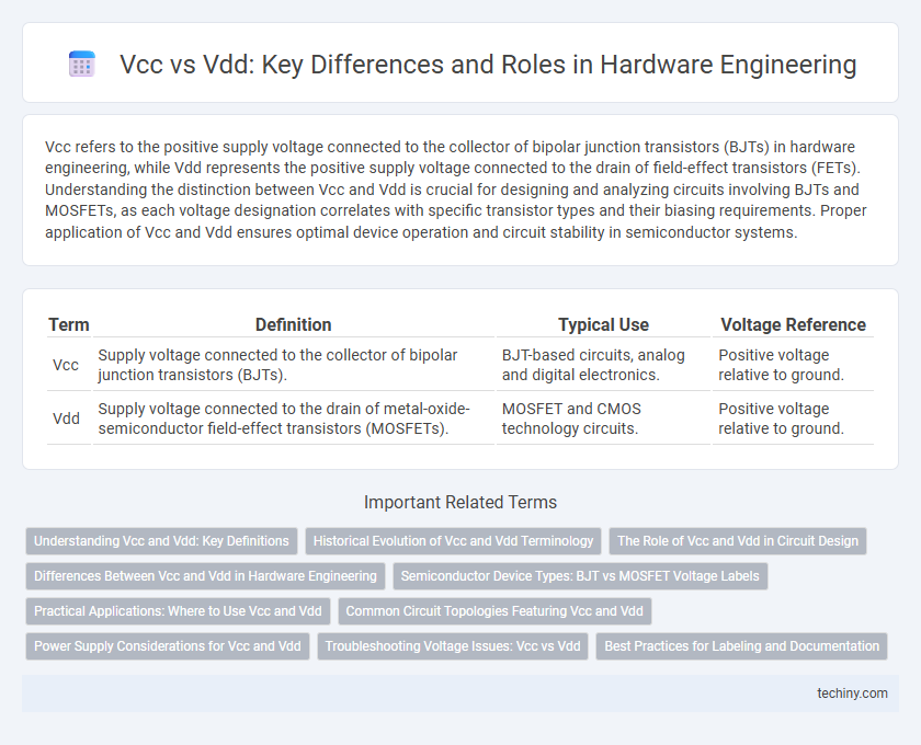
Vcc refers to the positive supply voltage connected to the collector of bipolar junction transistors (BJTs) in hardware engineering, while Vdd represents the positive supply voltage connected to the drain of field-effect transistors (FETs). Understanding the distinction between Vcc and Vdd is crucial for designing and analyzing circuits involving BJTs and MOSFETs, as each voltage designation correlates with specific transistor types and their biasing requirements. Proper application of Vcc and Vdd ensures optimal device operation and circuit stability in semiconductor systems.
Table of Comparison
| Term | Definition | Typical Use | Voltage Reference |
|---|---|---|---|
| Vcc | Supply voltage connected to the collector of bipolar junction transistors (BJTs). | BJT-based circuits, analog and digital electronics. | Positive voltage relative to ground. |
| Vdd | Supply voltage connected to the drain of metal-oxide-semiconductor field-effect transistors (MOSFETs). | MOSFET and CMOS technology circuits. | Positive voltage relative to ground. |
Understanding Vcc and Vdd: Key Definitions
Vcc and Vdd are essential voltage supply terminals in hardware engineering, where Vcc typically represents the positive supply voltage connected to the collector of bipolar junction transistors (BJTs), while Vdd refers to the positive supply voltage connected to the drain of field-effect transistors (FETs). Understanding Vcc and Vdd is crucial for designing and analyzing electronic circuits, as these voltages determine the operating conditions and power requirements of semiconductor devices. Precise identification of Vcc and Vdd ensures proper circuit functionality and prevents damage due to incorrect voltage application.
Historical Evolution of Vcc and Vdd Terminology
Vcc and Vdd terminology originated from early transistor circuits, where Vcc denoted the supply voltage connected to the collector of bipolar junction transistors (BJTs), and Vdd referred to the supply voltage connected to the drain of metal-oxide-semiconductor field-effect transistors (MOSFETs). As semiconductor technology evolved, these terms became standard references for power supply pins, with Vcc associated with positive supply in BJT circuits and Vdd in MOSFET-based digital integrated circuits. The historical evolution reflects the transition from bipolar to CMOS technologies, embedding Vcc and Vdd into hardware engineering lexicon for design clarity.
The Role of Vcc and Vdd in Circuit Design
Vcc and Vdd serve as critical voltage supply nodes in circuit design, where Vcc typically represents the positive supply voltage connected to the collector of bipolar junction transistors (BJTs), while Vdd denotes the positive voltage supply linked to the drain of field-effect transistors (FETs). Understanding the distinction between Vcc and Vdd is essential for optimizing power distribution and ensuring proper transistor operation within integrated circuits. Accurate identification of these voltages influences device reliability, switching performance, and overall circuit stability in hardware engineering.
Differences Between Vcc and Vdd in Hardware Engineering
Vcc refers to the supply voltage connected to the collector of bipolar junction transistors (BJTs), typically representing the positive power rail in circuits using BJTs. Vdd denotes the supply voltage connected to the drain of field-effect transistors (FETs), specifically MOSFETs, serving as the positive power supply in CMOS technology. Understanding the distinction between Vcc (BJT-based circuits) and Vdd (MOSFET-based circuits) is critical for accurate circuit design and power management in hardware engineering.
Semiconductor Device Types: BJT vs MOSFET Voltage Labels
Vcc and Vdd refer to voltage labels commonly used in semiconductor device circuits, with Vcc typically associated with Bipolar Junction Transistors (BJTs) representing the collector supply voltage, while Vdd corresponds to Metal-Oxide-Semiconductor Field-Effect Transistors (MOSFETs) indicating the drain supply voltage. BJTs operate with current-controlled junctions where Vcc signifies the positive supply relative to the emitter, whereas MOSFETs use voltage-controlled channels with Vdd marking the positive rail relative to the source. Understanding these voltage labels is crucial for correct circuit design and biasing in hardware engineering applications involving these semiconductor devices.
Practical Applications: Where to Use Vcc and Vdd
Vcc is commonly used to denote the positive supply voltage connected to the collector of bipolar junction transistors in analog and mixed-signal circuits, making it ideal for applications involving BJTs or older TTL logic devices. Vdd represents the positive supply voltage connected to the drain of MOSFET transistors, which is prevalent in modern CMOS digital circuits and microprocessors. Selecting Vcc or Vdd depends on the transistor technology employed, ensuring proper biasing and optimal device performance in hardware designs.
Common Circuit Topologies Featuring Vcc and Vdd
Common circuit topologies featuring Vcc and Vdd include bipolar junction transistor (BJT) amplifiers, where Vcc typically supplies the collector voltage, and CMOS logic gates, where Vdd provides the positive power rail to PMOS transistors. In BJT configurations like the common-emitter amplifier, Vcc establishes the necessary collector bias, while in complementary metal-oxide-semiconductor (CMOS) circuits, Vdd and ground define the voltage swing for digital logic levels. Understanding the roles of Vcc and Vdd in these topologies is essential for designing stable and efficient analog and digital integrated circuits.
Power Supply Considerations for Vcc and Vdd
Vcc and Vdd are critical power supply nodes in hardware engineering, representing the voltage supply for bipolar junction transistors (BJT) and MOSFET devices, respectively. Vcc typically refers to the positive voltage supply in BJT circuits, commonly at +5V or +12V, while Vdd denotes the drain supply voltage in MOSFET-based CMOS technology, often at lower voltages like +3.3V or +1.8V to reduce power consumption. Proper selection and regulation of Vcc and Vdd are essential to ensure device reliability, minimize noise, and optimize power efficiency in integrated circuits and mixed-signal applications.
Troubleshooting Voltage Issues: Vcc vs Vdd
Vcc and Vdd represent supply voltages in hardware engineering, often causing confusion during troubleshooting of voltage issues. Vcc refers to the voltage connected to the collector of bipolar junction transistors (BJTs), typically positive voltage, while Vdd denotes the drain supply voltage in field-effect transistors (FETs), usually the main positive power rail. Identifying whether a component uses Vcc or Vdd is crucial for diagnosing power faults, ensuring correct voltage measurements, and preventing damage from incorrect voltage application.
Best Practices for Labeling and Documentation
Label Vcc and Vdd clearly and consistently in schematics and PCB layouts to avoid confusion between voltage supply nodes, as Vcc typically refers to the positive supply for bipolar junction transistors and Vdd for MOSFETs. Use standardized naming conventions aligned with industry standards such as IEEE to facilitate communication among engineers and maintenance teams. Provide detailed annotations in documentation that specify voltage levels, reference points, and operating conditions to enhance clarity and ensure accurate hardware troubleshooting and modifications.
Vcc vs Vdd Infographic