DIP (Dual In-line Package) components feature through-hole leads that facilitate manual soldering and prototyping, making them suitable for low-volume production and repair. SMD (Surface-Mount Device) components offer a compact footprint and higher density assembly by mounting directly onto the PCB surface, optimizing space and enabling automated manufacturing. Choosing between DIP and SMD depends on factors such as design complexity, production scale, and assembly capabilities.
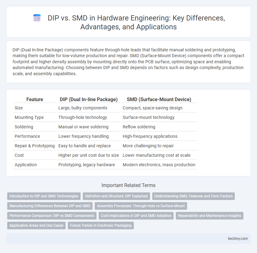
Table of Comparison
| Feature | DIP (Dual In-line Package) | SMD (Surface-Mount Device) |
|---|---|---|
| Size | Large, bulky components | Compact, space-saving design |
| Mounting Type | Through-hole technology | Surface-mount technology |
| Soldering | Manual or wave soldering | Reflow soldering |
| Performance | Lower frequency handling | High-frequency applications |
| Repair & Prototyping | Easy to handle and replace | More challenging to repair |
| Cost | Higher per unit cost due to size | Lower manufacturing cost at scale |
| Application | Prototyping, legacy hardware | Modern electronics, mass production |
Introduction to DIP and SMD Technologies
Dual In-line Package (DIP) technology features through-hole mounting where component leads pass through the PCB and are soldered on the opposite side, providing robust mechanical connections and ease of manual assembly. Surface-Mount Device (SMD) technology uses components mounted directly onto the PCB surface via soldering, enabling higher component density and improved performance in miniaturized hardware designs. Understanding the distinctions between DIP and SMD technologies is crucial for optimizing PCB layout, assembly techniques, and overall device reliability in hardware engineering.
Definition and Structure: DIP Explained
Dual In-line Package (DIP) is a through-hole mounting technology characterized by two parallel rows of pins extending perpendicularly from a rectangular plastic housing, allowing secure insertion into PCB holes. This electronic component package offers robust mechanical stability and ease of manual soldering, making it ideal for prototyping and low-volume production. The structure supports components such as integrated circuits and resistors, ensuring reliable electrical connections with printed circuit boards.
Understanding SMD: Features and Form Factors
Surface-Mount Devices (SMD) feature compact sizes and are designed for direct placement on PCB surfaces, enabling higher component density and automated assembly processes compared to Dual In-line Packages (DIP). Common SMD form factors include SOIC, QFN, and BGA, each offering unique benefits such as reduced parasitic inductance, improved thermal performance, and enhanced electrical characteristics. Understanding these form factors helps hardware engineers optimize circuit design for miniaturization and improved manufacturing reliability.
Manufacturing Differences Between DIP and SMD
DIP (Dual In-line Package) components require through-hole mounting, involving manual insertion and wave soldering, which increases assembly time and labor costs. SMD (Surface Mount Device) components enable automated pick-and-place assembly with reflow soldering, significantly improving production speed and accuracy. The surface mount technology facilitates miniaturization and higher component density on PCBs compared to the bulkier DIP format.
Assembly Processes: Through-Hole vs Surface-Mount
Through-hole assembly involves inserting component leads into pre-drilled holes on a PCB, providing strong mechanical bonds ideal for high-stress applications, while surface-mount device (SMD) assembly places components directly onto the PCB surface, enabling higher component density and faster automated production. Through-hole components typically require wave soldering or manual soldering, whereas SMD parts use reflow soldering techniques that offer improved precision and efficiency in mass manufacturing. The choice between through-hole and surface-mount assembly processes depends on factors like mechanical strength requirements, production volume, and PCB design constraints.
Performance Comparison: DIP vs SMD Components
DIP components typically offer better mechanical robustness and easier manual soldering, making them ideal for prototyping and repair, while SMD components excel in high-frequency performance due to their reduced parasitic inductance and capacitance. SMD technology supports higher component density and improved thermal performance, enabling faster signal processing and reduced electromagnetic interference. Overall, SMD components deliver superior performance in miniaturized, high-speed circuits, whereas DIP is preferred for applications requiring durability and straightforward handling.
Cost Implications in DIP and SMD Adoption
DIP (Dual In-line Package) components typically incur higher manufacturing and assembly costs due to manual handling and through-hole mounting processes. SMD (Surface-Mount Device) adoption reduces production expenses significantly by enabling automated placement and soldering, lowering labor and material costs. Bulk procurement of SMD components further decreases cost per unit, making SMDs more economically viable for large-scale hardware engineering projects.
Repairability and Maintenance Insights
Dual In-line Package (DIP) components offer superior repairability and ease of maintenance due to their through-hole mounting, allowing for straightforward desoldering and replacement with standard tools. Surface-Mount Device (SMD) components, while enabling compact designs, require specialized equipment like hot air rework stations for effective removal and repair, increasing maintenance complexity. Technicians often prefer DIP in prototyping and low-volume repairs, whereas SMD suits high-density production despite challenging serviceability.
Application Areas and Use Cases
DIP (Dual In-line Package) components are widely used in prototyping, educational kits, and through-hole PCB designs where ease of manual soldering and replacement is crucial. SMD (Surface-Mount Device) components dominate in high-density, compact electronics like smartphones, laptops, and automotive control systems due to their smaller size and suitability for automated assembly. Industrial machinery, consumer electronics, and telecommunications equipment leverage SMDs for enhanced performance, while DIP remains preferred for applications requiring robustness and straightforward hardware debugging.
Future Trends in Electronic Packaging
Surface-mount devices (SMD) continue to dominate electronic packaging due to their compact size and superior performance in high-frequency applications, enabling finer pitch and higher component density on printed circuit boards (PCBs). Dual in-line packages (DIP), while easier to prototype and debug, face declining usage as electronics trend toward miniaturization and automated assembly processes. Future trends emphasize the growth of advanced packaging technologies like system-in-package (SiP) and 3D integration, which build upon SMD advantages to enhance thermal management and signal integrity in increasingly complex hardware designs.
DIP vs SMD Infographic