Bare die offers superior thermal performance and reduced signal parasitics compared to packaged ICs, making it ideal for high-frequency and high-power applications. Packaged ICs provide mechanical protection, ease of handling, and standardized interfacing, which simplifies assembly and increases reliability in mass production. Choosing between bare die and packaged IC depends on application requirements such as thermal management, size constraints, and manufacturing complexity.
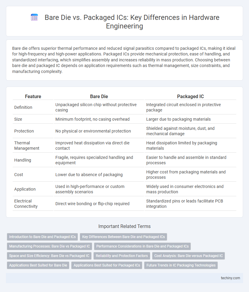
Table of Comparison
| Feature | Bare Die | Packaged IC |
|---|---|---|
| Definition | Unpackaged silicon chip without protective casing | Integrated circuit enclosed in protective package |
| Size | Minimum footprint, no casing overhead | Larger due to packaging materials |
| Protection | No physical or environmental protection | Shielded against moisture, dust, and mechanical damage |
| Thermal Management | Improved heat dissipation via direct die contact | Heat dissipation limited by packaging materials |
| Handling | Fragile, requires specialized handling and equipment | Easier to handle and assemble in standard processes |
| Cost | Lower due to absence of packaging | Higher cost from packaging materials and processes |
| Application | Used in high-performance or custom assembly scenarios | Widely used in consumer electronics and mass production |
| Electrical Connectivity | Direct wire bonding or flip-chip required | Standardized pins or leads facilitate PCB integration |
Introduction to Bare Die and Packaged ICs
Bare die refers to the raw semiconductor chip that contains integrated circuits without protective packaging, offering direct access to the silicon substrate for high-performance or specialized applications. Packaged ICs encase the bare die within a protective shell, providing mechanical support, heat dissipation, and standardized electrical connections for easier integration into electronic systems. The choice between bare die and packaged ICs depends on factors such as thermal management, assembly processes, and application-specific reliability requirements.
Key Differences Between Bare Die and Packaged ICs
Bare die refers to the raw semiconductor chip without any protective casing, offering direct access to the silicon surface and allowing for custom testing and integration in advanced hardware engineering applications. Packaged ICs encase the bare die within a protective enclosure, providing enhanced durability, standard connectivity through pins or pads, and simplified handling during assembly processes. The key differences include protection level, ease of handling, thermal management, and susceptibility to physical damage, where bare die favors customization and compactness while packaged ICs prioritize reliability and convenience.
Manufacturing Processes: Bare Die vs Packaged IC
Bare die manufacturing involves fabricating semiconductor chips directly on the wafer, followed by dicing without additional protective encapsulation. Packaged ICs undergo further processes such as wire bonding, molding, and encapsulation to protect the die and facilitate easier handling and integration into electronic systems. The choice between bare die and packaged IC manufacturing impacts thermal management, assembly complexity, and reliability in hardware engineering applications.
Performance Considerations in Bare Die and Packaged ICs
Bare die ICs offer lower parasitic capacitance and resistance, resulting in higher signal integrity and faster switching speeds compared to packaged ICs. Packaged ICs introduce additional inductance and thermal resistance through the package leads and substrate, potentially limiting maximum operating frequency and heat dissipation efficiency. Performance-critical applications such as high-frequency RF circuits or ultrafast processors benefit from the minimal electrical and thermal barriers present in bare die configurations.
Space and Size Efficiency: Bare Die vs Packaged IC
Bare die offers superior space and size efficiency compared to packaged ICs due to the absence of protective casing and leads, which allows direct integration onto substrates or PCB surfaces. This compact footprint significantly reduces parasitic inductance and capacitance, enhancing high-frequency performance in aerospace and satellite hardware applications. Packaged ICs, while providing mechanical protection and ease of handling, incur additional volume that can be critical in size-constrained hardware engineering designs.
Reliability and Protection Factors
Bare die offers superior thermal performance and reduced parasitic inductance, enhancing reliability in high-frequency applications but is more susceptible to environmental damage without encapsulation. Packaged ICs provide robust protection against moisture, mechanical stress, and electrostatic discharge, significantly improving long-term device reliability in harsh operating conditions. Selecting between bare die and packaged IC depends on the specific reliability requirements and protection factors dictated by the target hardware environment.
Cost Analysis: Bare Die versus Packaged IC
Bare die offers lower unit costs by eliminating packaging materials and assembly processes, making it cost-effective for high-volume production runs. Packaged ICs incur higher expenses due to encapsulation, testing, and protection, which add to manufacturing complexity and increase per-unit price. Cost analysis must consider volume, reliability requirements, and integration needs to determine the optimal choice between bare die and packaged IC.
Applications Best Suited for Bare Die
Bare die are best suited for high-density, space-constrained applications requiring direct die attachment to substrates, such as in advanced microelectromechanical systems (MEMS) and high-frequency RF modules. They enable superior thermal performance and reduced parasitic inductance, crucial for high-speed computing and power management integrated circuits. Bare die also facilitate custom packaging solutions in aerospace, medical implants, and specialized instrumentation where size and reliability are critical.
Applications Best Suited for Packaged ICs
Packaged ICs are best suited for applications requiring robust environmental protection, ease of handling, and simplified integration onto printed circuit boards (PCBs). They provide superior mechanical stability and thermal management, making them ideal for consumer electronics, automotive systems, and industrial equipment. Packaged ICs also enhance reliability in high-volume manufacturing environments due to standardized form factors and encapsulation materials.
Future Trends in IC Packaging Technologies
Future trends in IC packaging technologies emphasize the integration of bare die over traditional packaged ICs to enhance performance and reduce size. Advanced heterogeneous integration and 3D packaging methods enable higher interconnect density and improved thermal management. These innovations drive the development of more efficient, compact, and scalable hardware systems crucial for emerging applications like AI, 5G, and IoT devices.
bare die vs packaged IC Infographic