Clock skew refers to the deterministic difference in timing between clock signals arriving at different components, which can cause setup and hold time violations in synchronous circuits. Clock jitter, on the other hand, represents the random variation or noise in the clock signal timing that leads to unpredictable shifts in clock edges. Minimizing both clock skew and jitter is critical in hardware engineering to ensure reliable synchronization and optimal performance of digital systems.
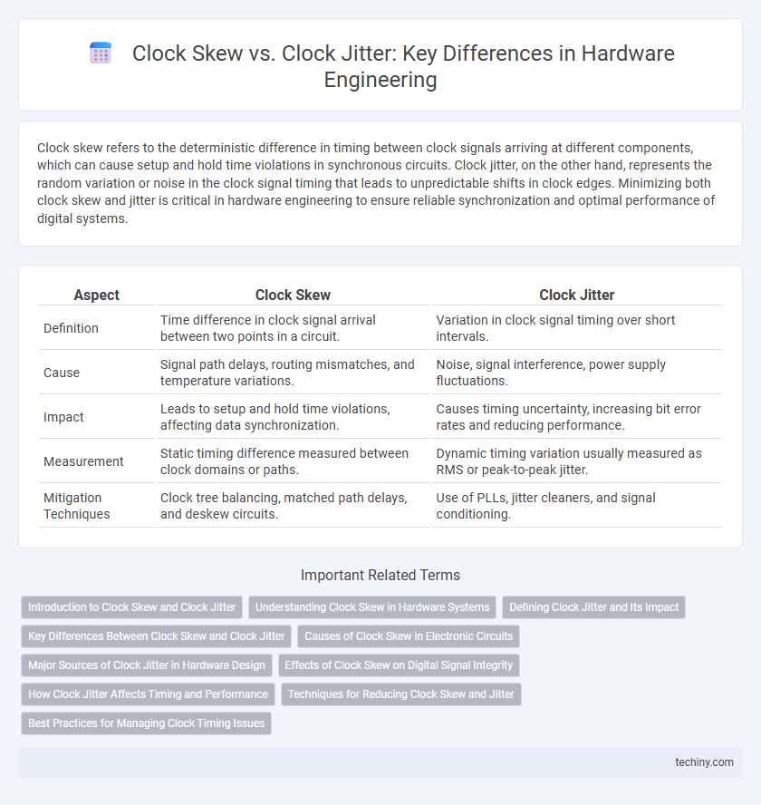
Table of Comparison
| Aspect | Clock Skew | Clock Jitter |
|---|---|---|
| Definition | Time difference in clock signal arrival between two points in a circuit. | Variation in clock signal timing over short intervals. |
| Cause | Signal path delays, routing mismatches, and temperature variations. | Noise, signal interference, power supply fluctuations. |
| Impact | Leads to setup and hold time violations, affecting data synchronization. | Causes timing uncertainty, increasing bit error rates and reducing performance. |
| Measurement | Static timing difference measured between clock domains or paths. | Dynamic timing variation usually measured as RMS or peak-to-peak jitter. |
| Mitigation Techniques | Clock tree balancing, matched path delays, and deskew circuits. | Use of PLLs, jitter cleaners, and signal conditioning. |
Introduction to Clock Skew and Clock Jitter
Clock skew refers to the difference in arrival times of the same clock signal at different components within a synchronous circuit, impacting timing accuracy and potentially causing setup or hold time violations. Clock jitter is the variation in the clock signal's timing from its ideal periodicity, introducing uncertainty in signal synchronization and affecting overall system performance. Understanding the distinction between clock skew and clock jitter is critical for optimizing timing closure and ensuring reliable hardware design in high-speed digital systems.
Understanding Clock Skew in Hardware Systems
Clock skew in hardware systems refers to the timing difference in signal arrival times between multiple clock signals distributed across a circuit, causing synchronization challenges in digital designs. Precise management of clock skew is essential to ensure reliable data transfer and to prevent race conditions in complex integrated circuits. Techniques such as clock tree synthesis and phase-locked loops are commonly employed to minimize skew and maintain system stability.
Defining Clock Jitter and Its Impact
Clock jitter refers to the variation in the timing of clock signal edges from their ideal positions, causing uncertainty in signal transitions within hardware circuits. This timing inconsistency can degrade the performance of high-speed digital systems by introducing errors in data sampling and synchronization. Managing clock jitter is critical to maintaining signal integrity and ensuring reliable operation in hardware engineering designs.
Key Differences Between Clock Skew and Clock Jitter
Clock skew refers to the difference in timing arrival of a clock signal at different components within a circuit, typically measured in nanoseconds, while clock jitter describes the short-term variations or timing fluctuations of the clock signal itself around its ideal position. Skew impacts synchronization across the circuit by causing data to arrive at uneven times, whereas jitter affects signal integrity and timing accuracy, potentially leading to data errors. Understanding these distinctions is crucial for designing reliable hardware systems, as managing skew involves layout and routing strategies, whereas jitter reduction focuses on improving clock source stability and signal conditioning.
Causes of Clock Skew in Electronic Circuits
Clock skew in electronic circuits arises primarily from variations in signal path delays, caused by differences in wire lengths, buffer stages, and load capacitances within the clock distribution network. Thermal gradients and manufacturing process variations also contribute to timing mismatches between clock signals reaching different components. These factors lead to misalignment of clock edges, affecting synchronization and overall circuit performance.
Major Sources of Clock Jitter in Hardware Design
Major sources of clock jitter in hardware design include power supply noise, electromagnetic interference (EMI), and thermal fluctuations, all of which cause timing variations in clock signals. Variations in voltage levels and substrate coupling can introduce random jitter that disrupts precise timing synchronization. Understanding these noise contributors is critical for optimizing PLL design and ensuring stable clock distribution networks in high-frequency systems.
Effects of Clock Skew on Digital Signal Integrity
Clock skew causes timing mismatches between clock signals arriving at different components, leading to setup and hold time violations that degrade digital signal integrity. It can induce metastability in flip-flops, resulting in unpredictable logic states and increased error rates. Managing clock skew is critical in synchronous circuits to maintain reliable data transfer and overall system performance.
How Clock Jitter Affects Timing and Performance
Clock jitter introduces variability in the timing of clock edges, causing uncertainty in signal synchronization and data capture. This timing variability can lead to setup and hold time violations in flip-flops and other sequential elements, reducing the reliability of high-speed digital circuits. Excessive clock jitter degrades overall system performance by increasing bit error rates and limiting the maximum achievable clock frequency in hardware designs.
Techniques for Reducing Clock Skew and Jitter
Techniques for reducing clock skew and jitter in hardware engineering involve using phase-locked loops (PLLs) and delay-locked loops (DLLs) to synchronize clock signals across circuits, minimizing timing discrepancies. Implementing balanced clock tree synthesis (CTS) ensures even distribution of clock signals, reducing skew by matching path delays. Employing low-jitter clock sources and signal conditioning, such as filtering and shielding, further enhances clock stability and accuracy in high-speed designs.
Best Practices for Managing Clock Timing Issues
Effective management of clock skew and clock jitter in hardware engineering involves precise timing analysis and synchronization techniques to minimize data corruption and signal integrity problems. Utilizing phase-locked loops (PLLs) and deskew circuits helps align clock signals across components, ensuring reliable system performance. Implementing rigorous layout designs, such as matched trace lengths and controlled impedance, reduces variability in clock propagation delays and mitigates timing uncertainties.
Clock Skew vs Clock Jitter Infographic