Leaded packages feature metal leads extending from the component body, facilitating easier soldering and inspection on printed circuit boards (PCBs), making them ideal for prototyping and designs requiring mechanical strength. Leadless packages eliminate external leads, reducing package size and parasitic inductance, which enhances high-frequency performance and enables better thermal dissipation. Choosing between leaded and leadless packages depends on application requirements such as assembly processes, electrical performance, and space constraints in hardware engineering.
Table of Comparison
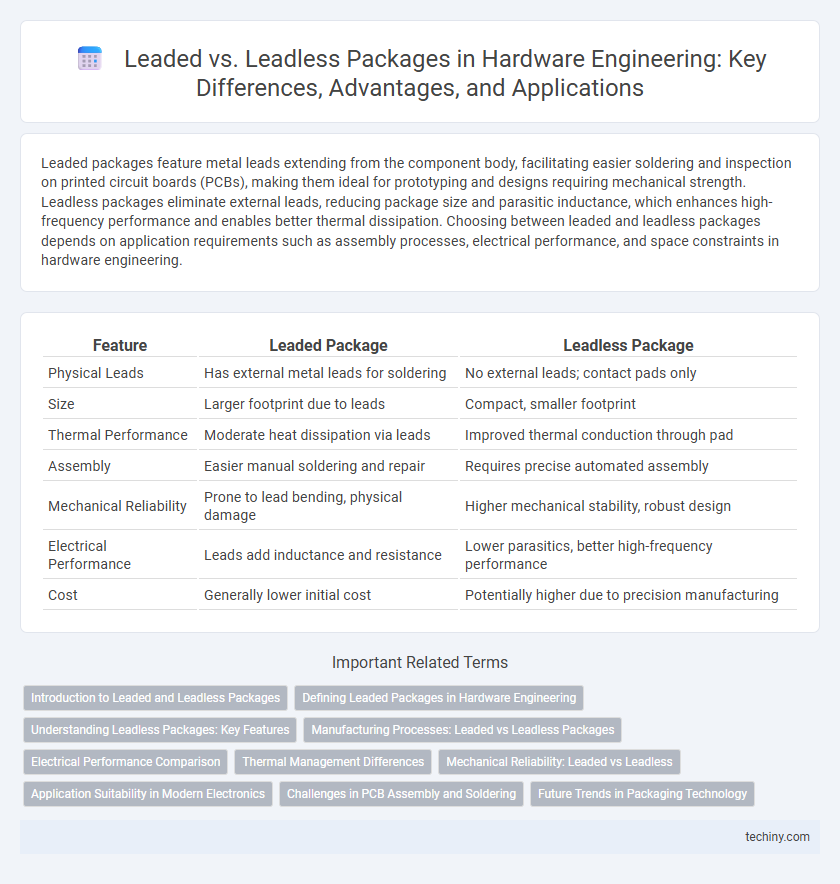
| Feature | Leaded Package | Leadless Package |
|---|---|---|
| Physical Leads | Has external metal leads for soldering | No external leads; contact pads only |
| Size | Larger footprint due to leads | Compact, smaller footprint |
| Thermal Performance | Moderate heat dissipation via leads | Improved thermal conduction through pad |
| Assembly | Easier manual soldering and repair | Requires precise automated assembly |
| Mechanical Reliability | Prone to lead bending, physical damage | Higher mechanical stability, robust design |
| Electrical Performance | Leads add inductance and resistance | Lower parasitics, better high-frequency performance |
| Cost | Generally lower initial cost | Potentially higher due to precision manufacturing |
Introduction to Leaded and Leadless Packages
Leaded packages feature external metal leads extending from the component body, facilitating manual soldering and prototyping in hardware engineering applications. Leadless packages, in contrast, eliminate external leads and use solder pads or terminals directly on the package surface, enabling higher component density and enhanced thermal performance on printed circuit boards (PCBs). The choice between leaded and leadless packages impacts assembly methods, mechanical durability, and electrical characteristics in circuit design.
Defining Leaded Packages in Hardware Engineering
Leaded packages in hardware engineering are electronic components encased with metal leads extending from the body, facilitating easy soldering onto printed circuit boards (PCBs). These leads provide reliable mechanical support and electrical connectivity, commonly found in Dual In-line Packages (DIP), Small Outline Integrated Circuits (SOIC), and Quad Flat Packages (QFP). The defined lead geometry simplifies prototype assembly and repair, making leaded packages preferred in applications requiring robust physical connections and manual soldering processes.
Understanding Leadless Packages: Key Features
Leadless packages in hardware engineering eliminate traditional metal leads, utilizing contact pads on the package surface for electrical connections, which enhances signal integrity and reduces parasitic inductance. These packages offer improved thermal performance and smaller footprints, making them ideal for high-density PCB designs. Common leadless types include QFN (Quad Flat No-lead) and DFN (Dual Flat No-lead), widely used in RF and power applications due to their reliability and cost-effectiveness.
Manufacturing Processes: Leaded vs Leadless Packages
Leaded packages involve inserting component leads into through-holes on printed circuit boards (PCBs), requiring wave soldering or selective soldering during manufacturing. Leadless packages use surface-mount technology (SMT), where components are directly placed on PCB pads and soldered using reflow soldering, enabling higher component density and automated assembly. The manufacturing process for leadless packages reduces material use and improves thermal performance but demands precise placement and advanced inspection techniques.
Electrical Performance Comparison
Leaded packages typically offer superior electrical performance due to longer pin lengths that provide better signal integrity and reduced parasitic inductance compared to leadless packages. The exposed leads in leaded packages enable easier testing and lower contact resistance, which enhances high-frequency operation and thermal dissipation. Conversely, leadless packages benefit from shorter signal paths that reduce inductive effects but may exhibit slightly higher contact resistance impacting high-speed circuit performance.
Thermal Management Differences
Leaded packages typically offer better thermal dissipation due to the presence of metal leads that facilitate heat transfer away from the semiconductor die. In contrast, leadless packages rely on the package substrate and soldering pads for thermal conduction, often resulting in higher junction temperatures if not properly designed. Optimizing thermal management in leadless packages involves advanced PCB design techniques, such as thermal vias and copper pours, to enhance heat spreading efficiency.
Mechanical Reliability: Leaded vs Leadless
Leaded packages provide enhanced mechanical reliability through their robust leads, which absorb stress and reduce solder joint fatigue during thermal cycling. Leadless packages, such as QFN or BGA, rely on direct solder connections to PCB pads, offering improved electrical performance but increased sensitivity to mechanical stress and potential joint cracking under vibration or flex. Mechanical reliability in leadless designs can be improved with optimized PCB layout, underfill materials, and controlled assembly processes.
Application Suitability in Modern Electronics
Leaded packages remain suitable for applications requiring robust mechanical connections and ease of prototyping in industrial and automotive electronics. Leadless packages excel in high-density, miniaturized consumer electronics due to their compact size and improved electrical performance. Modern electronics favor leadless designs for mobile devices and wearables, while leaded packages persist in environments demanding durability and straightforward repairability.
Challenges in PCB Assembly and Soldering
Leaded packages present challenges in PCB assembly due to the risk of solder bridging between leads, requiring precise alignment and solder paste application to prevent defects. Leadless packages, such as QFN or DFN, demand meticulous solder paste printing and inspection techniques because their solder joints are located beneath the component, making visual inspection difficult. Both package types require tailored reflow profiles to achieve optimal solder joint quality while minimizing warpage and component damage during the soldering process.
Future Trends in Packaging Technology
Future trends in hardware engineering emphasize leadless packaging due to its superior thermal performance, miniaturization capability, and environmental benefits in compliance with RoHS directives. Leaded packages face challenges adapting to high-density designs and automated assembly processes, driving the industry's shift toward leadless solutions such as QFN and BGA formats. Advances in materials and manufacturing techniques continue to enable higher reliability and electrical performance in leadless packages, positioning them as the dominant standard in next-generation electronic device packaging.
Leaded Package vs Leadless Package Infographic