Plated through holes (PTHs) provide robust electrical connections across multiple layers of a printed circuit board (PCB) and are essential for mounting through-hole components, offering mechanical strength and durability. Vias are smaller, plated holes that create electrical pathways between specific layers of a PCB without accommodating component leads, optimizing space and enabling high-density circuit designs. Choosing between PTHs and vias depends on the mechanical support requirements and the complexity of the PCB layout.
Table of Comparison
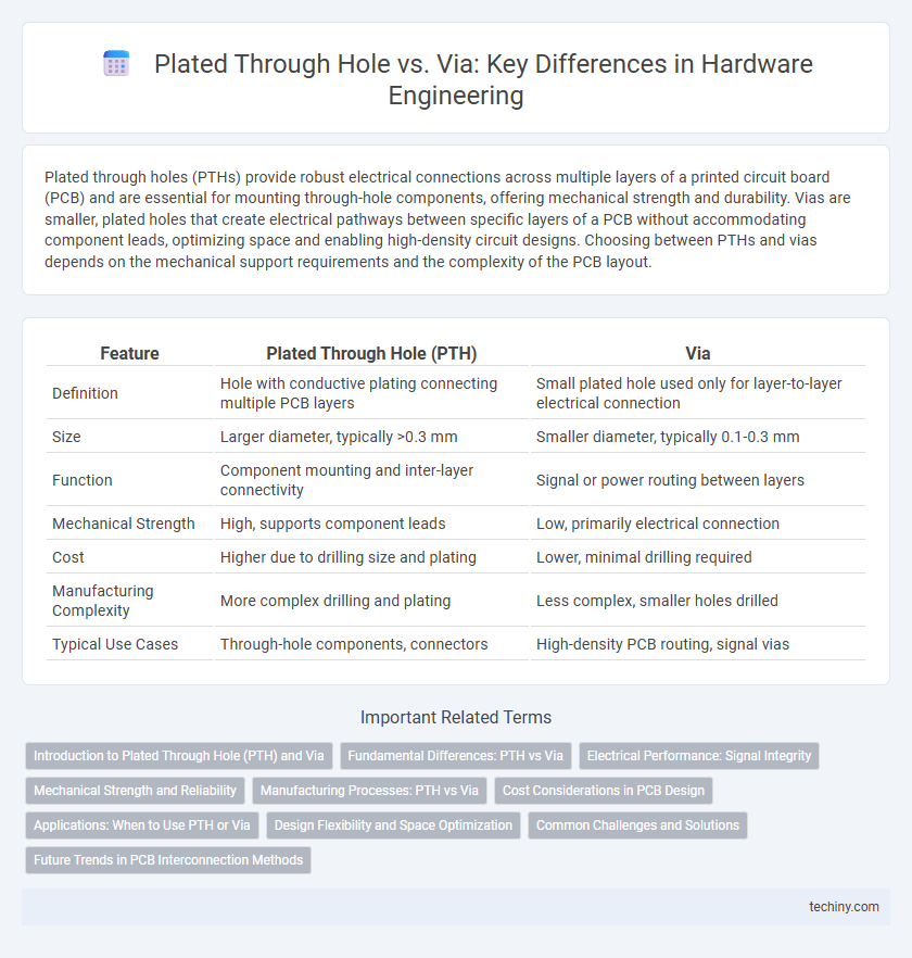
| Feature | Plated Through Hole (PTH) | Via |
|---|---|---|
| Definition | Hole with conductive plating connecting multiple PCB layers | Small plated hole used only for layer-to-layer electrical connection |
| Size | Larger diameter, typically >0.3 mm | Smaller diameter, typically 0.1-0.3 mm |
| Function | Component mounting and inter-layer connectivity | Signal or power routing between layers |
| Mechanical Strength | High, supports component leads | Low, primarily electrical connection |
| Cost | Higher due to drilling size and plating | Lower, minimal drilling required |
| Manufacturing Complexity | More complex drilling and plating | Less complex, smaller holes drilled |
| Typical Use Cases | Through-hole components, connectors | High-density PCB routing, signal vias |
Introduction to Plated Through Hole (PTH) and Via
A Plated Through Hole (PTH) is a drilled hole in a printed circuit board (PCB) that is plated with a conductive material to create an electrical connection between multiple layers. Vias are a specific type of PTH used primarily for establishing electrical pathways between PCB layers, typically smaller in diameter and not designed for component mounting. Both are essential in multilayer PCB design, enabling complex routing and efficient use of board space.
Fundamental Differences: PTH vs Via
Plated Through Holes (PTH) are drilled holes in a printed circuit board (PCB) that are coated with a conductive layer to create electrical connections between all layers they pass through, often used for component leads and mechanical support. Vias are smaller, strategically placed drilled holes that electrically connect specific PCB layers but do not accommodate component leads, primarily focusing on signal routing and layer interconnection. The fundamental difference lies in size, function, and application: PTHs support component mounting and reliable mechanical connections, whereas vias provide efficient interlayer electrical pathways without contributing to structural strength.
Electrical Performance: Signal Integrity
Plated through holes (PTH) provide robust mechanical and electrical connections by extending through the entire PCB, ensuring consistent signal transmission for high-current applications. Vias, typically smaller and used for signal routing between layers, introduce parasitic inductance and capacitance that can degrade signal integrity at high frequencies. Optimizing via design, including size, length, and placement, minimizes signal reflections and crosstalk, enhancing overall electrical performance in high-speed hardware engineering.
Mechanical Strength and Reliability
Plated through holes (PTHs) offer superior mechanical strength compared to vias due to their larger diameter and fully metallized barrel, enabling better support for heavy component leads and through-hole mounting. Vias, typically smaller and thinner, primarily facilitate electrical connections between PCB layers but provide less mechanical reinforcement, which can affect long-term reliability under mechanical stress. Employing PTHs in load-bearing areas enhances durability and reduces failure risks in complex hardware designs requiring robust structural integrity.
Manufacturing Processes: PTH vs Via
Plated Through Holes (PTH) involve drilling holes through the entire PCB thickness and electroplating the interior to create a conductive path, typically used for mounting through-hole components. Vias are smaller in diameter, drilled partially through the board layers, and serve primarily for electrical connections between different layers without accommodating component leads. Manufacturing processes for PTH require more material removal and plating, leading to longer cycle times and higher costs compared to vias, which are optimized for compact, multilayer PCBs with faster production workflows.
Cost Considerations in PCB Design
Plated through holes (PTH) generally incur higher costs than vias due to their larger size and more extensive drilling requirements, impacting material and manufacturing expenses in PCB design. Vias, typically smaller and used for interlayer connections, offer cost efficiency but may limit current capacity and mechanical strength compared to PTH. Balancing cost considerations with electrical performance and reliability demands careful selection between PTH and via implementations in multilayer PCB fabrication.
Applications: When to Use PTH or Via
Plated Through Holes (PTH) are ideal for mechanical support and strong electrical connections in multilayer printed circuit boards, commonly used for mounting through-hole components and connectors. Vias are primarily employed for electrically connecting different layers within a PCB, enabling compact designs and high-density interconnections in advanced hardware engineering. Choosing PTH is beneficial when component stability and durability are crucial, while vias optimize space and signal routing in complex multi-layer circuits.
Design Flexibility and Space Optimization
Plated through holes (PTH) provide robust mechanical and electrical connections across multiple PCB layers, supporting higher current loads but occupying more space due to their larger size. Vias offer enhanced design flexibility by enabling high-density routing with minimal footprint, ideal for space-optimized, multi-layer circuit boards. Utilizing a combination of PTH and vias allows hardware engineers to balance mechanical strength with space-efficient layouts, optimizing both performance and board real estate.
Common Challenges and Solutions
Plated through holes (PTHs) and vias both facilitate electrical connections between PCB layers but pose challenges such as reliability issues due to thermal stress and potential for cracks during soldering. Common solutions include optimizing plating thickness, improving hole wall cleanliness, and selecting appropriate materials to enhance adhesion and conductivity. Employing advanced inspection techniques like X-ray and automated optical inspection (AOI) helps detect defects early, ensuring integrity and performance in hardware engineering designs.
Future Trends in PCB Interconnection Methods
Future trends in PCB interconnection methods emphasize the evolution from traditional plated through holes (PTH) to advanced via technologies such as microvias and blind/buried vias, enabling higher density and improved signal integrity. Innovations in laser drilling and additive manufacturing facilitate the creation of smaller, more precise vias, supporting faster data transmission and enhanced thermal management in compact hardware designs. Integration of embedded components and the use of novel materials further optimize interconnect reliability and performance in next-generation hardware engineering.
Plated through hole vs Via Infographic