Schematic capture involves creating a detailed electrical diagram that defines the connections and components of a circuit, serving as the blueprint for electronic design. PCB layout translates the schematic into a physical board design, positioning components and routing traces to ensure signal integrity and manufacturability. Effective hardware engineering requires seamless integration between schematic capture and PCB layout to optimize performance and reliability.
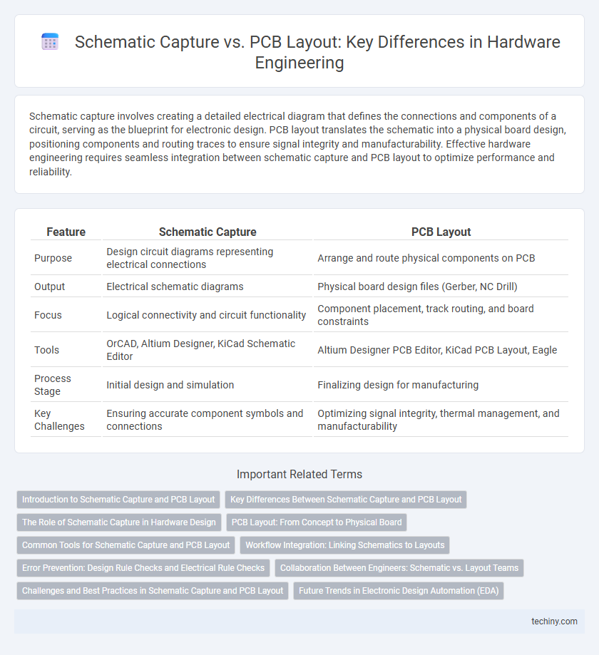
Table of Comparison
| Feature | Schematic Capture | PCB Layout |
|---|---|---|
| Purpose | Design circuit diagrams representing electrical connections | Arrange and route physical components on PCB |
| Output | Electrical schematic diagrams | Physical board design files (Gerber, NC Drill) |
| Focus | Logical connectivity and circuit functionality | Component placement, track routing, and board constraints |
| Tools | OrCAD, Altium Designer, KiCad Schematic Editor | Altium Designer PCB Editor, KiCad PCB Layout, Eagle |
| Process Stage | Initial design and simulation | Finalizing design for manufacturing |
| Key Challenges | Ensuring accurate component symbols and connections | Optimizing signal integrity, thermal management, and manufacturability |
Introduction to Schematic Capture and PCB Layout
Schematic capture is the foundational process in hardware engineering that involves creating an electrical diagram representing circuit connections and components. PCB layout translates the schematic into a physical design by arranging components and routing electrical paths on a printed circuit board. Mastery of both ensures accurate electrical functionality and manufacturability of electronic devices.
Key Differences Between Schematic Capture and PCB Layout
Schematic capture involves creating an abstract, symbolic representation of an electronic circuit, focusing on the electrical connections and component functions. PCB layout translates the schematic into a physical design by positioning components and routing copper traces on the board, considering factors like signal integrity and manufacturability. The key differences lie in schematic capture emphasizing circuit functionality and logic, whereas PCB layout prioritizes physical arrangement and electrical performance on the final printed circuit board.
The Role of Schematic Capture in Hardware Design
Schematic capture serves as the foundational step in hardware design by translating circuit concepts into detailed electronic diagrams, enabling precise component interconnections and functionality verification before physical implementation. It ensures accurate netlist generation, which is critical for seamless PCB layout and reduces errors during manufacturing. This process enhances design clarity, supports simulation and validation, and streamlines collaboration among engineering teams.
PCB Layout: From Concept to Physical Board
PCB layout transforms the schematic design into a physical board by defining component placement, routing signal traces, and ensuring electrical performance and manufacturability. Key considerations include optimizing trace impedance, minimizing crosstalk, adhering to design for manufacturability (DFM) guidelines, and managing thermal dissipation. Advanced PCB layout software integrates design rule checks (DRC), 3D visualization, and real-time error detection to streamline the transition from concept to physical hardware.
Common Tools for Schematic Capture and PCB Layout
Popular tools for schematic capture and PCB layout include Altium Designer, Eagle, and KiCad, which offer integrated environments for designing electronic circuits and printed circuit boards. These tools provide robust libraries of components, simulation capabilities, and real-time design rule checks to optimize circuit integrity and manufacturability. Users benefit from seamless transitions between schematic capture and PCB layout phases, ensuring accurate signal routing and component placement.
Workflow Integration: Linking Schematics to Layouts
Schematic capture serves as the foundational step in hardware design, where circuit diagrams are created with precise component symbols and interconnections. PCB layout translates these schematics into physical board designs, focusing on component placement, routing, and electrical constraints. Seamless workflow integration ensures that changes in the schematic automatically update the PCB layout, maintaining design consistency and accelerating the engineering process.
Error Prevention: Design Rule Checks and Electrical Rule Checks
Design Rule Checks (DRCs) in PCB layout automatically enforce physical constraints such as trace widths, spacing, and component clearances to prevent manufacturing errors. Electrical Rule Checks (ERCs) in schematic capture validate connectivity, ensuring signal integrity by detecting issues like unconnected pins, short circuits, and incorrect voltage levels. Combining DRC and ERC in hardware engineering workflows significantly reduces design errors, improves reliability, and streamlines the transition from schematic to PCB fabrication.
Collaboration Between Engineers: Schematic vs. Layout Teams
Effective collaboration between schematic capture and PCB layout teams hinges on clear communication and shared design data, enabling seamless translation of circuit intent into physical board architecture. Utilizing integrated design tools and version control systems minimizes errors and streamlines iterative feedback between electrical engineers and layout specialists. This synergy enhances design accuracy, reduces time-to-market, and ensures compliance with electrical and manufacturing constraints.
Challenges and Best Practices in Schematic Capture and PCB Layout
Effective schematic capture requires precise symbol management and clear net labeling to prevent errors during PCB layout, addressing challenges like component misplacement and signal integrity issues. Best practices include using hierarchical design methods, regular design rule checks (DRC), and thorough peer reviews to ensure accuracy and consistency between schematic and layout. In PCB layout, managing trace impedance, minimizing crosstalk, and optimizing component placement for thermal performance are critical to achieving functional, manufacturable circuit boards.
Future Trends in Electronic Design Automation (EDA)
Schematic capture and PCB layout are evolving with artificial intelligence and machine learning integration, enabling automated error detection and intelligent component placement to enhance design accuracy and reduce development time. Cloud-based EDA platforms facilitate real-time collaboration and version control, streamlining complex hardware engineering projects and accelerating innovation cycles. Advanced simulation tools and predictive analytics are improving design validation processes, ensuring higher reliability and performance in future electronic systems.
Schematic capture vs PCB layout Infographic