Schematic design represents the logical connection of electronic components, serving as a blueprint for circuit functionality, while layout design translates this schematic into a physical arrangement of components on a printed circuit board (PCB). The schematic ensures correct electrical connectivity, and the layout addresses spatial constraints, signal integrity, and manufacturability. Precision in both schematic and layout stages is critical for successful hardware engineering and optimal device performance.
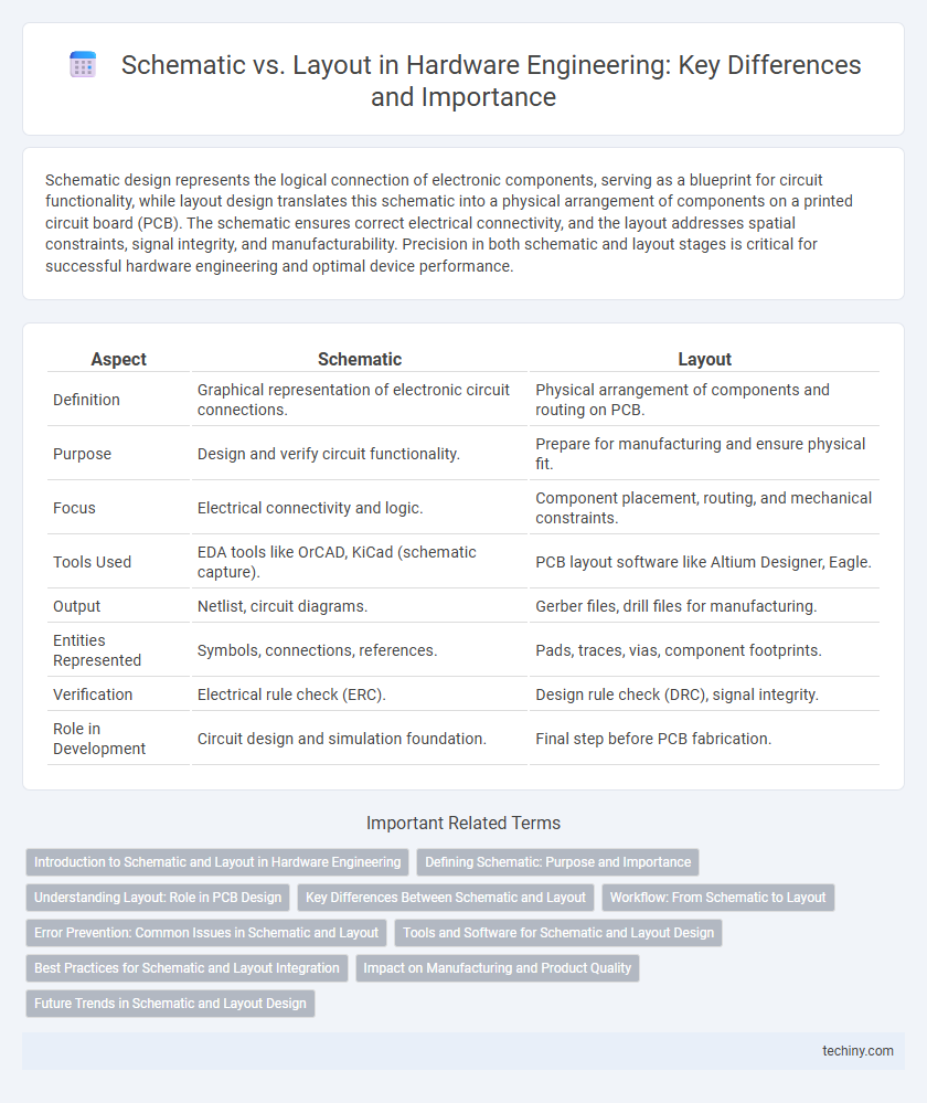
Table of Comparison
| Aspect | Schematic | Layout |
|---|---|---|
| Definition | Graphical representation of electronic circuit connections. | Physical arrangement of components and routing on PCB. |
| Purpose | Design and verify circuit functionality. | Prepare for manufacturing and ensure physical fit. |
| Focus | Electrical connectivity and logic. | Component placement, routing, and mechanical constraints. |
| Tools Used | EDA tools like OrCAD, KiCad (schematic capture). | PCB layout software like Altium Designer, Eagle. |
| Output | Netlist, circuit diagrams. | Gerber files, drill files for manufacturing. |
| Entities Represented | Symbols, connections, references. | Pads, traces, vias, component footprints. |
| Verification | Electrical rule check (ERC). | Design rule check (DRC), signal integrity. |
| Role in Development | Circuit design and simulation foundation. | Final step before PCB fabrication. |
Introduction to Schematic and Layout in Hardware Engineering
Schematic design in hardware engineering involves creating a detailed diagram that represents the electrical connections and components within a circuit, serving as the blueprint for the system's functionality. Layout design translates the schematic into the physical placement of components and routing of electrical traces on a printed circuit board (PCB), optimizing space and signal integrity. Both stages are crucial for ensuring the prototype's performance, manufacturability, and reliability in electronic device production.
Defining Schematic: Purpose and Importance
The schematic serves as the fundamental blueprint in hardware engineering, illustrating the electrical connections and components in a circuit. It defines the functional design, enabling engineers to analyze and verify circuit behavior before physical implementation. Accurate schematics are crucial for effective communication, troubleshooting, and ensuring the integrity of the final hardware layout.
Understanding Layout: Role in PCB Design
In PCB design, the layout is crucial for translating the schematic into a physical board by defining the precise placement of components and routing of electrical connections. It ensures signal integrity, thermal management, and manufacturability while minimizing noise and interference. Effective layout design directly impacts the performance, reliability, and durability of the hardware system.
Key Differences Between Schematic and Layout
Schematic diagrams represent the electrical connections and components of a circuit using standardized symbols, focusing on functionality and logical design. Layout refers to the physical placement and routing of components on a printed circuit board (PCB), emphasizing spatial arrangement and manufacturability. Key differences include the schematic's role in circuit design verification versus the layout's role in ensuring signal integrity, thermal management, and compliance with manufacturing constraints.
Workflow: From Schematic to Layout
The workflow from schematic to layout begins with capturing the circuit design using schematic software, defining all components and their electrical connections. After validating the schematic for design rule compliance and functionality, engineers transfer the netlist to layout tools, where physical placement and routing occur based on the schematic's connectivity data. This transition ensures accurate representation of electrical relationships while optimizing the physical design for performance, manufacturability, and signal integrity.
Error Prevention: Common Issues in Schematic and Layout
Schematic errors often stem from incorrect symbol connections or missing components, leading to functional faults in the circuit design. Layout issues typically involve trace routing problems such as short circuits, signal integrity disturbances, or insufficient spacing causing manufacturing defects. Implementing rigorous Design Rule Checks (DRC) and Electrical Rule Checks (ERC) early in the design process minimizes these errors, ensuring accurate translation from schematic to physical board layout.
Tools and Software for Schematic and Layout Design
Schematic design tools such as Altium Designer, OrCAD Capture, and Eagle provide intuitive interfaces for creating and editing circuit diagrams, enabling precise component symbol placement and netlist generation. Layout software like Altium Designer, Mentor Graphics PADS, and KiCad converts schematics into physical PCB layouts, offering advanced features for trace routing, layer management, and design rule checks. Integration between schematic capture and layout environments ensures seamless data transfer and synchronization, enhancing accuracy and efficiency in hardware engineering workflows.
Best Practices for Schematic and Layout Integration
Ensuring seamless schematic and layout integration involves maintaining consistent component naming and precise netlist verification to prevent design discrepancies. Utilizing design rule checks (DRCs) within the EDA tools helps identify potential layout errors aligned with schematic constraints early in the process. Implementing hierarchical design methodologies and version control systems ensures synchronization between schematic updates and physical layout changes, reducing iteration cycles and improving design accuracy.
Impact on Manufacturing and Product Quality
Schematic design defines the electrical connections and functional intent, directly influencing manufacturability by ensuring clear communication of circuit requirements to production teams. Layout translates the schematic into physical placement of components and routing, critically affecting signal integrity, thermal management, and assembly precision, which all impact product quality. Optimizing both schematic and layout phases reduces manufacturing errors and enhances reliability, resulting in superior end-product performance and lower defect rates.
Future Trends in Schematic and Layout Design
Emerging trends in schematic and layout design emphasize enhanced integration of AI-driven automation tools that optimize circuit accuracy and reduce design cycle times. Advanced simulation techniques leveraging machine learning improve predictive analysis for signal integrity and power distribution in complex systems. The convergence of 3D IC layout methodologies with schematic capture streamlines multi-die connectivity, enabling higher performance and miniaturization in next-generation hardware engineering.
Schematic vs Layout Infographic