Bonding wire connects semiconductor chips to their package leads through fine metal wires, offering flexibility and easier rework but with higher inductance and larger footprint. Flip chip technology directly attaches the chip to the substrate via solder bumps, providing superior electrical performance, reduced parasitic resistance, and smaller package size. While bonding wire is cost-effective for low to medium volume production, flip chip is preferred for high-density, high-frequency applications demanding enhanced thermal management.
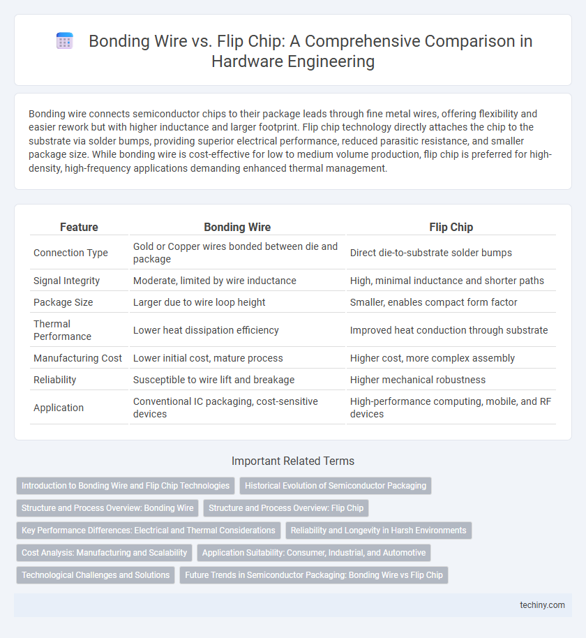
Table of Comparison
| Feature | Bonding Wire | Flip Chip |
|---|---|---|
| Connection Type | Gold or Copper wires bonded between die and package | Direct die-to-substrate solder bumps |
| Signal Integrity | Moderate, limited by wire inductance | High, minimal inductance and shorter paths |
| Package Size | Larger due to wire loop height | Smaller, enables compact form factor |
| Thermal Performance | Lower heat dissipation efficiency | Improved heat conduction through substrate |
| Manufacturing Cost | Lower initial cost, mature process | Higher cost, more complex assembly |
| Reliability | Susceptible to wire lift and breakage | Higher mechanical robustness |
| Application | Conventional IC packaging, cost-sensitive devices | High-performance computing, mobile, and RF devices |
Introduction to Bonding Wire and Flip Chip Technologies
Bonding wire technology involves using fine metal wires, typically gold or copper, to create electrical connections between the semiconductor chip and the package leads, offering proven reliability and flexibility in design. Flip chip technology directly mounts the chip face-down onto the substrate using solder bumps, enabling shorter electrical paths, improved performance, and enhanced thermal management in high-density applications. Both methods are critical in hardware engineering for optimizing signal integrity, power efficiency, and manufacturing scalability based on specific device requirements.
Historical Evolution of Semiconductor Packaging
Bonding wire technology, pioneered in the mid-20th century, revolutionized semiconductor packaging by enabling reliable electrical connections between the die and the package, driving the growth of microelectronics. Flip chip packaging emerged in the 1960s as a solution to overcome the speed and performance limitations of bonding wires, offering shorter interconnect paths and higher input/output density. The evolution from bonding wire to flip chip reflects the semiconductor industry's shift towards miniaturization, improved thermal management, and enhanced electrical performance in advanced electronic devices.
Structure and Process Overview: Bonding Wire
Bonding wire technology uses fine metal wires, typically gold or copper, to connect the semiconductor die to the package leads, creating an electrical path through a physical loop structure. The process involves ultrasonic or thermosonic welding to attach the wire bonds onto the die pads and lead frame, requiring precise alignment and controlled force to ensure reliable connections. This method contrasts with flip chip assembly by maintaining the die in an upright position and providing flexibility in wire routing for complex packaging designs.
Structure and Process Overview: Flip Chip
Flip chip technology uses solder bumps on the die surface to create direct electrical connections with the substrate, enabling a shorter signal path and improved electrical performance compared to traditional bonding wire. The process involves fabricating microscopic bumps on the chip pads, flipping the chip to align these bumps with the substrate pads, and then reflow soldering to establish the connections. This structure eliminates wire loops, reduces parasitic inductance, and supports higher input/output densities, making it ideal for advanced, high-performance semiconductor packaging.
Key Performance Differences: Electrical and Thermal Considerations
Bonding wire offers flexibility and ease of repair but presents higher electrical inductance and resistance compared to flip chip technology, which directly attaches the die to the substrate, significantly reducing signal path length and improving electrical performance. Flip chip also enhances thermal dissipation by eliminating the wire bond loop, allowing more efficient heat transfer through the substrate, critical for high-power applications. In summary, flip chip outperforms bonding wire in electrical signal integrity and thermal management, making it preferable for advanced high-frequency and high-power devices.
Reliability and Longevity in Harsh Environments
Bonding wire offers proven reliability in harsh environments due to its flexibility and ability to absorb mechanical stress, reducing risk of connection failures under thermal cycling and vibration. Flip chip technology provides superior electrical performance and compactness but requires robust underfill materials to enhance reliability and prevent solder joint fatigue in extreme conditions. For applications demanding prolonged durability in corrosive or high-temperature settings, bonding wire remains a dependable choice, whereas flip chip's longevity depends heavily on advanced packaging techniques and environmental controls.
Cost Analysis: Manufacturing and Scalability
Bonding wire technology offers lower initial manufacturing costs due to simpler equipment and established processes, making it suitable for low to medium volume production. Flip chip packaging involves higher upfront investment in advanced equipment and materials but provides superior scalability and cost efficiency for high-volume manufacturing by enabling smaller die sizes and higher interconnect densities. Economies of scale favor flip chip solutions as production volume increases, reducing per-unit costs despite higher initial expenditures.
Application Suitability: Consumer, Industrial, and Automotive
Bonding wire technology is widely used in consumer electronics due to its cost-effectiveness and ease of manufacturing, making it suitable for low to mid-range performance requirements. Flip chip packaging offers superior electrical performance and thermal management, making it ideal for demanding industrial applications and automotive systems that require high reliability and robust environmental tolerance. Both technologies serve distinct markets, with bonding wire favored for consumer devices and flip chip preferred in industrial and automotive sectors demanding enhanced durability and performance.
Technological Challenges and Solutions
Bonding wire faces challenges such as inductance limitations and signal integrity issues at high frequencies, which impact performance in advanced semiconductor packages. Flip chip technology addresses these problems by enabling shorter interconnects and improved electrical characteristics but demands precise alignment and advanced underfill materials to enhance reliability. Innovations in materials engineering and microfabrication have led to solutions like low-k dielectrics and optimized bump metallurgy to overcome thermal and mechanical stresses in flip chip assemblies.
Future Trends in Semiconductor Packaging: Bonding Wire vs Flip Chip
Future trends in semiconductor packaging emphasize advanced bonding wire materials such as copper and gold alloys to enhance electrical performance and reliability, while flip chip technology continues to evolve with finer pitch capabilities and increased integration density. Innovations in bonding wire aim to reduce parasitic inductance and improve thermal conductivity, making them suitable for high-frequency applications. Simultaneously, flip chip packaging advances support heterogeneous integration and 3D stacking, driving the development of compact, high-performance devices for AI, IoT, and 5G markets.
bonding wire vs flip chip Infographic