Boundary Scan provides a non-intrusive method for testing integrated circuits by shifting test data through a serial chain of boundary cells, improving fault isolation on PCBs. In-Circuit Test (ICT) physically probes the circuit nodes to check component values and connectivity, offering detailed fault detection at the cost of requiring physical access and handling. Combining Boundary Scan with ICT enhances test coverage and diagnostics in complex hardware systems, optimizing manufacturing quality and reducing time-to-market.
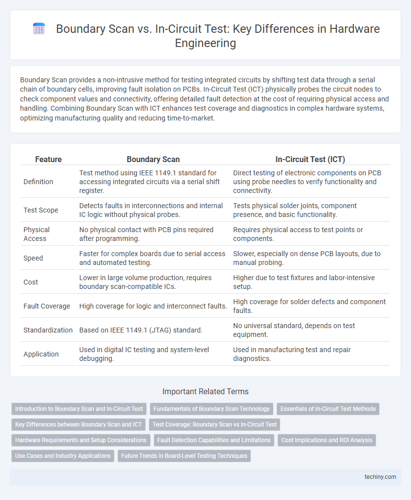
Table of Comparison
| Feature | Boundary Scan | In-Circuit Test (ICT) |
|---|---|---|
| Definition | Test method using IEEE 1149.1 standard for accessing integrated circuits via a serial shift register. | Direct testing of electronic components on PCB using probe needles to verify functionality and connectivity. |
| Test Scope | Detects faults in interconnections and internal IC logic without physical probes. | Tests physical solder joints, component presence, and basic functionality. |
| Physical Access | No physical contact with PCB pins required after programming. | Requires physical access to test points or components. |
| Speed | Faster for complex boards due to serial access and automated testing. | Slower, especially on dense PCB layouts, due to manual probing. |
| Cost | Lower in large volume production, requires boundary scan-compatible ICs. | Higher due to test fixtures and labor-intensive setup. |
| Fault Coverage | High coverage for logic and interconnect faults. | High coverage for solder defects and component faults. |
| Standardization | Based on IEEE 1149.1 (JTAG) standard. | No universal standard, depends on test equipment. |
| Application | Used in digital IC testing and system-level debugging. | Used in manufacturing test and repair diagnostics. |
Introduction to Boundary Scan and In-Circuit Test
Boundary Scan is a testing technique that uses a standardized IEEE 1149.1 protocol to access and control individual pins of integrated circuits for fault detection and diagnosis without physical test probes. In-Circuit Test (ICT) employs a bed of nails fixture to physically contact circuit nodes, measuring electrical parameters such as resistance, capacitance, and signal continuity to detect manufacturing defects. Both methods are essential for comprehensive hardware verification, with Boundary Scan offering non-intrusive testing mainly for complex PCBs and ICT providing detailed pin-level analysis.
Fundamentals of Boundary Scan Technology
Boundary Scan technology leverages the IEEE 1149.1 standard to enable testing of interconnects and internal circuitry without physical test probes, utilizing a shift-register architecture embedded in the chip. It facilitates fault detection by capturing data at the chip pins and allows for easier diagnosis of solder joint defects and board-level faults compared to traditional In-Circuit Test methods. This technology reduces test complexity and enhances fault coverage by enabling access to otherwise inaccessible nodes on densely packed hardware assemblies.
Essentials of In-Circuit Test Methods
In-circuit test (ICT) methods primarily focus on verifying the functionality and integrity of individual components on a printed circuit board (PCB) through direct electrical measurements such as resistance, capacitance, and signal continuity. ICT utilizes bed-of-nails fixtures to establish contact with test points, enabling detection of open circuits, short circuits, and component placement errors. Unlike boundary scan, which tests interconnects via serial data chains, ICT provides detailed diagnostics of component-level faults essential for early-stage hardware verification and manufacturing quality control.
Key Differences between Boundary Scan and ICT
Boundary Scan utilizes a standardized IEEE 1149.1 test access port to enable internal circuit testing without physical test probes, enhancing testing of densely packed PCBs and reducing test fixture costs. In-Circuit Test (ICT) physically probes individual test points on the PCB to measure electrical performance, allowing direct fault isolation but requiring complex fixtures and test setups. Boundary Scan excels in accessibility and automation for complex boards, while ICT provides detailed parametric measurements essential for comprehensive electrical validation.
Test Coverage: Boundary Scan vs In-Circuit Test
Boundary Scan provides high test coverage for interconnects and structural defects on printed circuit boards without physical probe access, enabling fault detection in inaccessible nodes. In-Circuit Test achieves comprehensive coverage by measuring electrical parameters at individual components, verifying solder joints and component values directly through test fixtures. Combining both methods enhances overall coverage by addressing limitations unique to each testing approach in hardware engineering.
Hardware Requirements and Setup Considerations
Boundary Scan requires minimal physical access to the device pins, enabling testability through standard JTAG interfaces with no need for custom test fixtures. In-Circuit Test demands extensive hardware setup, including dedicated test fixtures and bed-of-nails probes to physically access circuit nodes, increasing complexity and cost. Hardware requirements for Boundary Scan emphasize compliance with IEEE 1149.1 standards, while In-Circuit Test demands precise alignment and robust fixture design for reliable signal probing.
Fault Detection Capabilities and Limitations
Boundary Scan offers superior fault detection for interconnects and solder joints on complex printed circuit boards (PCBs) by enabling access to internal nodes and providing at-speed testing without physical probes. In-Circuit Test (ICT) excels at detecting component faults such as open pins, shorts, and incorrect values through direct electrical measurements but struggles with inaccessible or densely populated board areas. Limitations of Boundary Scan include reliance on built-in test structures and reduced efficiency for analog faults, whereas ICT is limited by fixture complexity and reduced coverage on high-density, multi-layer PCBs.
Cost Implications and ROI Analysis
Boundary Scan technology reduces test fixture expenses and shortens test setup time by enabling direct access to integrated circuit pins, leading to lower upfront costs compared to traditional In-Circuit Test (ICT) methods. While ICT offers comprehensive fault coverage, its higher equipment and maintenance costs can impact overall ROI, especially for low to medium volume production runs. Investing in Boundary Scan yields better cost-efficiency and faster ROI for complex, high-mix printed circuit board assemblies due to minimized physical test requirements and enhanced test automation.
Use Cases and Industry Applications
Boundary Scan is extensively used in aerospace and automotive industries for testing densely packed printed circuit boards (PCBs) where physical test access is limited. In-Circuit Test (ICT) is favored in mass production environments like consumer electronics manufacturing for rapid fault detection and component verification on accessible circuit boards. Both techniques complement each other, with Boundary Scan excelling in diagnosing failures in complex, multilayer PCBs while ICT provides high-speed, comprehensive electrical testing of individual components.
Future Trends in Board-Level Testing Techniques
Boundary scan technology is evolving with advancements in IEEE 1149.x standards, enabling enhanced access to embedded components for improved fault detection and diagnostics. In-circuit test (ICT) is integrating with automated optical inspection and machine learning algorithms to increase test coverage and reduce fault isolation time. The future of board-level testing is trending towards hybrid approaches combining boundary scan's structural insights and ICT's parametric measurements for comprehensive, efficient validation of complex electronic assemblies.
Boundary Scan vs In-Circuit Test Infographic