Chip-scale packages (CSP) offer a compact form factor by encapsulating a die in a package nearly the same size as the chip itself, enhancing electrical performance and thermal management in hardware engineering applications. Wafer-level packages (WLP) are fabricated directly on the wafer, enabling high-volume production and improved interconnect density without additional packaging steps. Comparing CSP and WLP reveals trade-offs in complexity, cost, and integration, crucial for optimizing electronic device assembly and functionality.
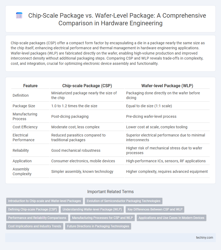
Table of Comparison
| Feature | Chip-scale Package (CSP) | Wafer-level Package (WLP) |
|---|---|---|
| Definition | Miniaturized package nearly the size of the chip | Packaging done directly on the wafer before dicing |
| Package Size | 1.0 to 1.2 times the die size | Equal to die size (1:1 scale) |
| Manufacturing Process | Post-dicing packaging | Pre-dicing wafer-level process |
| Cost Efficiency | Moderate cost, less complex | Lower cost at scale, complex tooling |
| Electrical Performance | Reduced parasitics compared to traditional packages | Superior electrical performance due to minimal interconnects |
| Reliability | Good mechanical robustness | Higher risk of mechanical stress due to wafer processes |
| Application | Consumer electronics, mobile devices | High-performance ICs, sensors, RF applications |
| Assembly Complexity | Simpler assembly, known technology | Higher complexity, requires advanced equipment |
Introduction to Chip-scale and Wafer-level Packages
Chip-scale packages (CSP) and wafer-level packages (WLP) are advanced semiconductor packaging technologies designed to enhance device performance and reduce form factor. CSP offers a compact footprint nearly the size of the semiconductor die, optimizing electrical performance and thermal management by minimizing interconnect length. WLP extends this concept by performing packaging directly on the wafer, enabling high-volume manufacturing efficiency and further miniaturization critical in modern electronics such as smartphones and wearable devices.
Evolution of Semiconductor Packaging Technologies
Chip-scale packages (CSP) represent a significant advancement from traditional wafer-level packages (WLP) by offering a smaller footprint and improved electrical performance through direct die attachment and redistribution layers. The evolution from WLP to CSP has enabled higher integration density and better thermal management, crucial for modern high-performance semiconductor devices. This progression in packaging technology supports enhanced miniaturization and reliability demands in advanced hardware engineering applications.
Defining Chip-scale Package (CSP)
Chip-scale Package (CSP) is a type of semiconductor packaging that closely matches the size of the integrated circuit die, typically less than 1.2 times the die area, providing a compact and efficient solution for high-density electronic designs. CSP offers improved electrical performance and thermal management compared to traditional packages by minimizing interconnect length and parasitic inductance. This packaging method is widely used in mobile devices and high-speed computing where space constraints and performance are critical.
Understanding Wafer-level Package (WLP)
Wafer-level Package (WLP) offers a compact and efficient semiconductor packaging solution by integrating the entire packaging process at the wafer level before dicing, significantly reducing package size and improving electrical performance. Unlike traditional Chip-scale Packages (CSP), WLP enables direct mounting on the printed circuit board (PCB) without additional substrates, enhancing thermal dissipation and signal integrity. This technology is essential for high-density applications in mobile devices and IoT products, where space constraints and electrical efficiency are critical.
Key Differences Between CSP and WLP
Chip-scale package (CSP) and wafer-level package (WLP) primarily differ in their manufacturing processes and form factors, with CSP being a small package assembled after wafer dicing, while WLP is fabricated directly on the wafer before dicing. CSP typically offers better mechanical robustness and easier integration onto printed circuit boards due to its standardized package shape, whereas WLP provides superior electrical performance and minimal package size by eliminating additional packaging layers. The choice between CSP and WLP influences assembly cost, thermal management, and signal integrity in advanced hardware engineering applications.
Performance and Reliability Comparisons
Chip-scale packages (CSP) offer enhanced electrical performance due to shorter interconnects and reduced parasitic inductance compared to wafer-level packages (WLP). Wafer-level packages provide superior thermal management and mechanical reliability by enabling uniform encapsulation and minimizing solder joint stress. Reliability assessments show CSP excels in high-frequency applications, while WLP's advantages lie in robust environmental stress resistance and improved heat dissipation.
Manufacturing Processes for CSP and WLP
Chip-scale package (CSP) manufacturing involves assembling and encapsulating the die with substrates, using wire bonding or flip-chip techniques to connect the integrated circuit to the package. Wafer-level package (WLP) manufacturing occurs at the wafer stage, applying redistribution layers, solder bumps, and final testing before dicing, enabling a more compact and cost-effective solution. CSP processes generally require additional steps after wafer dicing, while WLP integrates packaging steps directly on the wafer, enhancing throughput and reducing material usage.
Applications and Use Cases in Modern Devices
Chip-scale packages (CSP) are widely used in mobile devices and IoT sensors due to their compact size and enhanced electrical performance, enabling efficient space utilization on PCB layouts. Wafer-level packages (WLP) offer advantages in high-volume production environments for applications like smartphones and wearables, delivering superior thermal management and cost-effectiveness. Both packaging types support advanced semiconductor technologies, but CSP excels in performance-critical components while WLP is preferred for ultra-thin and flexible device integration.
Cost Implications and Industry Trends
Chip-scale packages (CSP) generally offer lower per-unit costs compared to wafer-level packages (WLP) due to simplified assembly and reduced material usage, making them favorable for high-volume consumer electronics. Wafer-level packaging, while initially more expensive due to advanced fabrication processes, provides superior performance and miniaturization benefits that are driving its adoption in premium and high-reliability applications. Industry trends indicate a growing shift towards WLP as advancements reduce costs and demand rises for compact, high-performance devices in mobile and wearable technology markets.
Future Directions in Packaging Technologies
Wafer-level packaging (WLP) advances by enabling higher I/O densities and improved thermal management through simultaneous wafer processing, fostering integration with system-in-package (SiP) solutions. Chip-scale packaging (CSP) is evolving to enhance miniaturization and electrical performance with new dielectric materials and advanced redistribution layers (RDLs). Future directions emphasize heterogeneous integration, incorporating 3D stacking and advanced interposers to meet demands for higher bandwidth and reduced form factors in next-generation semiconductor devices.
Chip-scale Package vs Wafer-level Package Infographic