Solder mask and paste mask serve distinct functions in hardware engineering; solder mask provides a protective layer that prevents oxidation and solder bridging on PCB surfaces, while paste mask defines precise areas for solder paste application during surface mount technology (SMT) assembly. Proper differentiation and application of these masks are critical for ensuring electrical insulation, component placement accuracy, and overall PCB reliability. Optimizing solder mask thickness and paste mask openings enhances solder joint quality and minimizes defects in electronic manufacturing.
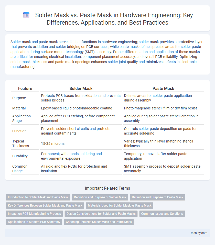
Table of Comparison
| Feature | Solder Mask | Paste Mask |
|---|---|---|
| Purpose | Protects PCB traces from oxidation and prevents solder bridges | Defines areas for solder paste application during assembly |
| Material | Epoxy-based liquid photoimageable coating | Photoimageable stencil film or dry film resist |
| Application Stage | Applied after PCB etching, before component placement | Applied during solder paste stencil creation in assembly |
| Function | Prevents solder short circuits and protects against contaminants | Controls solder paste deposition on pads for accurate soldering |
| Typical Thickness | 15-35 microns | Varies; typically thin layer matching stencil thickness |
| Durability | Permanent; withstands soldering and environmental exposure | Temporary; removed after solder paste application |
| Common Usage | All rigid and flex PCBs for protection and insulation | SMT assembly process to deposit solder paste accurately |
Introduction to Solder Mask and Paste Mask
Solder mask is a protective polymer layer applied to printed circuit boards (PCBs) to prevent solder bridges and protect copper traces from oxidation and environmental damage. Paste mask, also known as solder paste stencil, is a temporary resist layer used during the solder paste application process to define areas where solder is deposited for component placement. Both masks are critical in PCB manufacturing, with solder mask ensuring long-term durability and paste mask facilitating precise soldering during assembly.
Definition and Purpose of Solder Mask
Solder mask is a protective layer applied to printed circuit boards (PCBs) to prevent solder bridging and short circuits during the soldering process. It defines the areas where solder can be applied, enhancing the reliability and performance of electronic assemblies by insulating conductive traces. Unlike paste mask, which functions as a stencil for solder paste application during surface mount technology (SMT), solder mask primarily serves as a protective barrier to ensure precise soldering and protect against environmental damage.
Definition and Purpose of Paste Mask
Paste mask, also known as solder paste mask, is a stencil or layer applied on a PCB to define precise locations where solder paste is deposited for surface-mount device (SMD) assembly. Its primary purpose is to prevent solder paste from spreading to unwanted areas, ensuring accurate and efficient solder joint formation during reflow soldering. Unlike solder mask, which provides insulation and protection, paste mask specifically controls solder paste application to enhance component placement and soldering quality.
Key Differences Between Solder Mask and Paste Mask
Solder mask is a protective layer applied over the PCB to prevent solder bridging and environmental damage, while paste mask is a stencil or film used to define precise areas for solder paste application during surface-mount assembly. The solder mask is typically green and remains on the PCB permanently, enhancing durability and insulation, whereas the paste mask is temporary, guiding solder paste deposition for component placement. Key differences also include their functions: solder mask insulates exposed copper traces, while paste mask ensures accurate solder paste volume and placement, critical for reliable electrical connections.
Materials Used for Solder Mask vs Paste Mask
Solder mask typically utilizes epoxy liquid photoimageable materials that provide excellent insulation and protection against oxidation, while paste mask employs solder paste composed of metal alloy powders suspended in a flux medium designed to facilitate solder joint formation. The epoxy-based solder mask ensures durability and coverage over copper traces, whereas the solder paste mask's flux contains rosin or synthetic activators to enhance wetting and adhesion during reflow soldering. Material selection for solder mask focuses on chemical resistance and electrical insulation, whereas paste mask materials prioritize melting point and flux activity for proper solder application.
Impact on PCB Manufacturing Process
Solder mask and paste mask are critical in PCB manufacturing, with solder mask applied as a protective layer to prevent solder bridging and corrosion, thereby enhancing reliability and yield. Paste mask defines solder paste application areas for surface mount components, ensuring precise deposition and minimizing defects during reflow soldering. The interplay between these masks directly impacts solder joint quality, assembly accuracy, and overall production efficiency.
Design Considerations for Solder and Paste Masks
Design considerations for solder and paste masks center around ensuring proper adhesion, electrical insulation, and precision in component placement during PCB assembly. Solder masks require high thermal resistance and chemical stability to protect copper traces from oxidation and prevent solder bridging, while paste masks must provide accurate aperture definition for precise solder paste deposition to achieve reliable solder joints. Material compatibility, mask thickness, and resolution directly impact manufacturability and long-term performance of the PCB.
Common Issues and Solutions
Solder mask and paste mask defects commonly include misalignment, bridging, and insufficient coverage, which can lead to electrical shorts and poor solder joints. Addressing these issues involves precise mask registration, optimized stencil design, and consistent process controls during printing and curing stages. Implementing automated optical inspection (AOI) helps detect defects early, enabling corrective actions to maintain PCB quality and reliability.
Applications in Modern PCB Assembly
Solder masks provide a protective layer on PCBs to prevent oxidation and shorts, essential for high-reliability electronics in consumer, automotive, and aerospace sectors. Paste masks, also known as solder paste stencils, are critical in surface mount technology (SMT) processes for precise application of solder paste on pads, ensuring accurate component placement and solder joint quality. Modern PCB assembly integrates both masks to optimize manufacturing efficiency, reduce defects, and support high-density component layouts in advanced electronic devices.
Choosing Between Solder Mask and Paste Mask
Choosing between solder mask and paste mask depends on the specific requirements of the PCB assembly process. Solder mask provides a protective layer to prevent solder bridging and corrosion, ensuring insulation between conductive traces, while paste mask is used to define areas where solder paste is applied for component placement during reflow soldering. Evaluating factors such as component density, board complexity, and soldering method enables engineers to select the optimal mask to improve assembly accuracy and reliability.
Solder Mask vs Paste Mask Infographic