Microvias are small-diameter vias used to connect adjacent layers in high-density printed circuit boards (PCBs), offering superior electrical performance and space efficiency compared to blind vias. Blind vias connect outer layers to one or more inner layers but do not pass completely through the PCB, making them suitable for layered signal integrity while maintaining surface area. Microvias are typically created using laser drilling, enabling finer resolution and higher layer counts, which is critical for advanced hardware engineering applications.
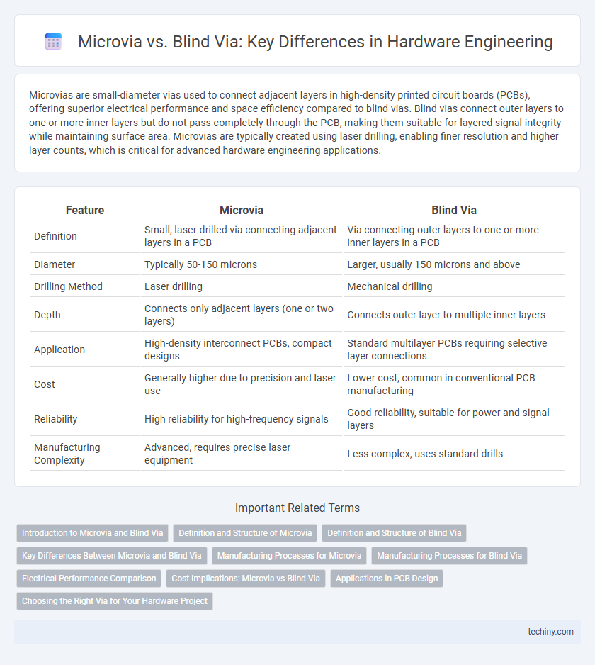
Table of Comparison
| Feature | Microvia | Blind Via |
|---|---|---|
| Definition | Small, laser-drilled via connecting adjacent layers in a PCB | Via connecting outer layers to one or more inner layers in a PCB |
| Diameter | Typically 50-150 microns | Larger, usually 150 microns and above |
| Drilling Method | Laser drilling | Mechanical drilling |
| Depth | Connects only adjacent layers (one or two layers) | Connects outer layer to multiple inner layers |
| Application | High-density interconnect PCBs, compact designs | Standard multilayer PCBs requiring selective layer connections |
| Cost | Generally higher due to precision and laser use | Lower cost, common in conventional PCB manufacturing |
| Reliability | High reliability for high-frequency signals | Good reliability, suitable for power and signal layers |
| Manufacturing Complexity | Advanced, requires precise laser equipment | Less complex, uses standard drills |
Introduction to Microvia and Blind Via
Microvias are tiny laser-drilled holes used in high-density interconnect (HDI) printed circuit boards (PCBs) to connect adjacent layers with diameters typically less than 150 microns. Blind vias connect outer layers to one or more inner layers without passing through the entire PCB, improving signal integrity and reducing board size. Microvias enable higher circuit density and better electrical performance compared to traditional blind vias due to their smaller size and precision placement.
Definition and Structure of Microvia
Microvias are small-diameter vias used in high-density interconnect (HDI) printed circuit boards (PCBs), typically laser-drilled and less than 150 microns in diameter, allowing electrical connections between adjacent layers. Unlike blind vias, which extend from the surface to an inner layer and may vary in size, microvias are limited in depth to one or two layers and provide more precise, reliable connections. The structure of a microvia consists of a thin, plated barrel filled or unfilled, optimized for minimal signal loss and improved electrical performance in compact PCB designs.
Definition and Structure of Blind Via
A blind via is a plated hole in a printed circuit board (PCB) that connects an outer layer to one or more inner layers without passing through the entire board, enhancing signal integrity and saving space in multi-layer designs. Structurally, a blind via is typically created by drilling from the surface layer and plating the hole walls to establish electrical connectivity between specified layers. Compared to microvias, which are smaller and often laser-drilled for high-density interconnects, blind vias generally have a larger diameter and are used for intermediate-layer connections in complex PCBs.
Key Differences Between Microvia and Blind Via
Microvias are small-diameter vias typically less than 150 microns deep, used to connect adjacent layers in high-density PCB designs, while blind vias connect an outer layer to one or more inner layers without passing through the entire board. Microvias are laser-drilled and preferred for fine-pitch applications due to their minimal aspect ratio, whereas blind vias are mechanically drilled and suited for less dense interconnections. The key differences lie in size, drilling method, and layer connectivity, impacting signal integrity and manufacturing complexity in multilayer printed circuit boards.
Manufacturing Processes for Microvia
Microvia manufacturing involves advanced laser drilling techniques to create small-diameter holes, typically less than 150 microns, enabling high-density interconnects in HDI PCBs. Unlike blind vias, which connect outer layers to one or more inner layers but require mechanical drilling, microvias use precise laser ablation to ensure minimal impact on surrounding substrates and greater reliability. This process facilitates thicker copper plating and tighter pitch layouts, crucial for modern compact electronic devices.
Manufacturing Processes for Blind Via
Blind vias in hardware engineering are created using precise laser drilling or mechanical drilling processes to connect outer and inner layers without penetrating the entire PCB thickness. The manufacturing process involves plating the drilled hole with copper to ensure reliable electrical conductivity and structural integrity. Compared to microvias, blind via fabrication requires more robust drilling techniques and thorough inspection to prevent defects such as incomplete plating or barrel defects.
Electrical Performance Comparison
Microvias offer superior electrical performance compared to blind vias due to their smaller size and reduced parasitic inductance, which minimizes signal loss and crosstalk in high-frequency applications. The shorter electrical path of microvias enhances signal integrity and reduces impedance discontinuities, crucial for high-speed printed circuit boards (PCBs). Blind vias, while effective for layer-to-layer connections, typically exhibit higher capacitance and resistance, leading to degraded signal quality in advanced hardware designs.
Cost Implications: Microvia vs Blind Via
Microvias generally offer lower cost implications compared to blind vias due to their smaller size, requiring less drilling time and material removal, which reduces manufacturing efforts and expenses. Blind vias involve deeper drilling and complex plating processes that increase production costs, particularly in multilayer PCB designs. Selecting microvias can optimize budget efficiency in high-density interconnects while maintaining performance and reliability standards.
Applications in PCB Design
Microvias enhance high-density PCB designs by enabling precise signal routing in compact multilayer boards, making them ideal for advanced applications like smartphones and aerospace electronics. Blind vias connect outer layers to one or more inner layers without passing through the entire PCB, optimizing space and improving signal integrity in moderate layer-count designs such as automotive and industrial control circuits. Both via types are crucial for managing signal integrity, thermal performance, and manufacturing cost in complex printed circuit board layouts.
Choosing the Right Via for Your Hardware Project
Microvias offer higher precision and are ideal for high-density PCB designs due to their smaller size and reduced signal interference, making them crucial for advanced hardware engineering projects. Blind vias connect outer layers to one or more inner layers without passing through the entire board, providing effective routing solutions for multilayer PCBs with moderate complexity. Selecting the right via depends on factors like board complexity, signal integrity requirements, manufacturing capabilities, and cost considerations to ensure optimal electrical performance and reliability.
Microvia vs Blind Via Infographic