PTH (Plated Through Hole) vias pass entirely through the PCB, providing robust electrical connections between multiple layers but occupying more space and potentially increasing parasitic inductance. Blind vias connect outer layers to one or more inner layers without traversing the entire board thickness, optimizing space usage and signal integrity in high-density designs. Choosing between PTH and blind vias impacts manufacturing complexity, cost, and overall board performance in multilayer hardware engineering applications.
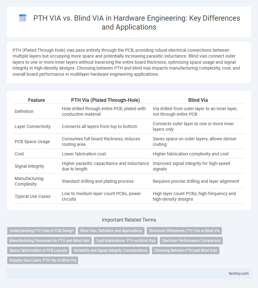
Table of Comparison
| Feature | PTH Via (Plated Through-Hole) | Blind Via |
|---|---|---|
| Definition | Hole drilled through entire PCB, plated with conductive material | Via drilled from outer layer to an inner layer, not through entire PCB |
| Layer Connectivity | Connects all layers from top to bottom | Connects outer layer to one or more inner layers only |
| PCB Space Usage | Consumes full board thickness, reduces routing area | Saves space on outer layers, allows denser routing |
| Cost | Lower fabrication cost | Higher fabrication complexity and cost |
| Signal Integrity | Higher parasitic capacitance and inductance due to length | Improved signal integrity for high-speed signals |
| Manufacturing Complexity | Standard drilling and plating process | Requires precise drilling and layer alignment |
| Typical Use Cases | Low to medium layer count PCBs, power circuits | High layer count PCBs, high-frequency and high-density designs |
Understanding PTH Vias in PCB Design
PTH vias, or Plated Through Holes, are essential in PCB design for establishing electrical connections between multiple layers by drilling holes completely through the board and plating them with conductive material. Unlike blind vias, which connect only outer layers to one or more inner layers without passing through the entire board, PTH vias provide robust structural support and reliable current carrying capacity across all layers. Optimizing PTH via placement enhances signal integrity and thermal management, making them a crucial consideration in advanced hardware engineering and multilayer PCB fabrication.
Blind Vias: Definition and Applications
Blind vias are plated-through holes that connect only outer layers to one or more inner layers on a printed circuit board (PCB), without passing completely through the substrate. They are essential in high-density interconnect (HDI) designs, enabling multi-layer routing while saving space and maintaining integrity in compact hardware systems. Common applications include advanced microelectronics, such as smartphones and medical devices, where PCB real estate and signal integrity are critical.
Structural Differences: PTH Via vs Blind Via
PTH (Plated Through-Hole) vias penetrate the entire PCB thickness, creating a continuous electrical connection across all layers, while blind vias only connect outer layers to one or more inner layers without passing through the entire board. The structural advantage of blind vias lies in their space-saving design since they do not occupy real estate on the opposite side of the PCB, allowing higher circuit density. This differentiation impacts manufacturing complexity, with PTH vias generally easier to produce but less efficient for high-density, multi-layered PCB designs.
Manufacturing Processes for PTH and Blind Vias
Manufacturing processes for PTH (Plated Through Hole) vias involve drilling holes completely through the PCB substrate followed by copper plating to establish electrical connections between all layers. Blind vias are created using laser or mechanical drilling techniques that penetrate only select layers without passing through the entire board, reducing signal interference and saving space. Both methods require precise drilling accuracy and controlled plating processes to ensure electrical reliability and mechanical stability in multilayer PCB assemblies.
Cost Implications: PTH vs Blind Vias
Plated Through-Hole (PTH) vias generally incur lower manufacturing costs compared to blind vias due to simpler drilling processes and less stringent alignment requirements. Blind vias, which connect outer layers to one or more inner layers without passing through the entire board, require advanced laser drilling or sequential lamination techniques, increasing fabrication expenses. The cost differential also reflects increased inspection complexity and potential yield reductions associated with blind via implementation in multilayer PCB designs.
Electrical Performance Comparison
PTH (Plated Through Hole) vias exhibit lower signal integrity for high-speed applications due to increased parasitic capacitance and inductance compared to blind vias, which have shorter electrical paths and reduced via stub effects. Blind vias improve electrical performance by minimizing signal reflection and crosstalk, enhancing impedance control and reducing insertion loss. This makes blind vias preferable for high-frequency circuits where maintaining signal integrity is critical.
Space Optimization in PCB Layouts
PTH vias penetrate the entire PCB thickness, enabling reliable layer-to-layer connections but consuming more board space compared to blind vias. Blind vias connect outer layers to inner layers without passing through the entire board, significantly optimizing space by allowing more compact routing in high-density PCB layouts. Utilizing blind vias enhances routing efficiency and maximizes available surface area, crucial for miniaturized hardware designs.
Reliability and Signal Integrity Considerations
PTH vias offer robust mechanical connections but introduce higher parasitic inductance and capacitance, potentially impacting signal integrity in high-speed circuits. Blind vias minimize signal path length and reduce via stubs, enhancing signal integrity by lowering signal reflections and crosstalk. Reliability of PTH vias is generally higher due to full-hole plating, whereas blind vias require precise manufacturing controls to avoid defects affecting long-term durability.
Choosing Between PTH and Blind Vias
Choosing between plated through-hole (PTH) vias and blind vias involves evaluating board space and signal integrity requirements. Blind vias connect outer layers to internal layers without passing through the entire PCB, reducing parasitic capacitance and preserving more routing area compared to PTH vias. Selecting blind vias enhances high-speed signal performance and miniaturization in complex multilayer boards, while PTH vias provide mechanical strength for components needing robust solder joints.
Industry Use Cases: PTH Via vs Blind Via
PTH vias, or plated through-hole vias, are extensively used in multilayer printed circuit boards (PCBs) for their reliable electrical connections that pass through the entire board, making them ideal for complex, high-density applications like automotive and aerospace electronics. Blind vias, which only connect outer layers to one or more inner layers without penetrating the entire board, optimize space and improve signal integrity in compact devices such as smartphones and advanced medical equipment where miniaturization is critical. Industry adoption of blind vias supports enhanced performance and reduced manufacturing costs by enabling finer routing and higher routing density compared to PTH vias, which remain preferred for mechanical stability and simpler fabrication processes.
PTH via vs Blind via Infographic