Schematic design provides a symbolic representation of the electronic circuit, highlighting the relationships and connections between components, essential for understanding circuit functionality. PCB layout translates the schematic into a physical design by placing components and routing electrical traces, optimizing for signal integrity and manufacturability. Effective hardware engineering requires seamless integration between schematics and PCB layouts to ensure performance, reliability, and adherence to design constraints.
Table of Comparison
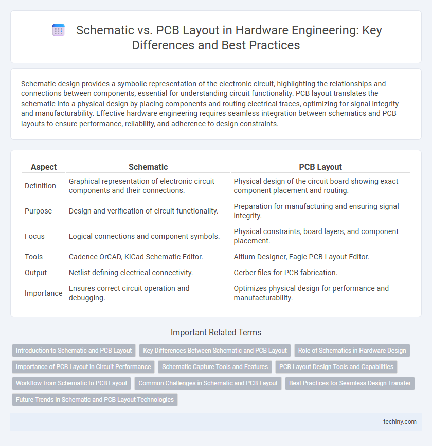
| Aspect | Schematic | PCB Layout |
|---|---|---|
| Definition | Graphical representation of electronic circuit components and their connections. | Physical design of the circuit board showing exact component placement and routing. |
| Purpose | Design and verification of circuit functionality. | Preparation for manufacturing and ensuring signal integrity. |
| Focus | Logical connections and component symbols. | Physical constraints, board layers, and component placement. |
| Tools | Cadence OrCAD, KiCad Schematic Editor. | Altium Designer, Eagle PCB Layout Editor. |
| Output | Netlist defining electrical connectivity. | Gerber files for PCB fabrication. |
| Importance | Ensures correct circuit operation and debugging. | Optimizes physical design for performance and manufacturability. |
Introduction to Schematic and PCB Layout
A schematic is a detailed diagram that represents the electrical connections and components within a circuit, serving as the blueprint for circuit functionality and design intent. PCB layout translates this schematic into a physical design, specifying the precise placement of components and routing of electrical pathways on the printed circuit board. Efficient collaboration between schematic creation and PCB layout optimization is crucial for minimizing signal interference, improving electrical performance, and ensuring manufacturability in hardware engineering projects.
Key Differences Between Schematic and PCB Layout
Schematic design represents the electrical connections and components in a symbolic diagram, focusing on circuit functionality and logical flow. PCB layout translates this schematic into a physical board design, detailing the placement of components and routing of copper traces to ensure manufacturability and signal integrity. Key differences include the schematic's abstract representation for circuit understanding, whereas the PCB layout addresses spatial constraints, electrical performance, and physical fabrication requirements.
Role of Schematics in Hardware Design
Schematics serve as the foundational blueprint in hardware engineering, detailing the electrical connections and component relationships essential for circuit functionality. They enable engineers to visualize and verify signal paths, component specifications, and system architecture before proceeding to PCB layout design. Accurate schematics ensure effective communication across design teams and form the basis for automated PCB routing and verification processes.
Importance of PCB Layout in Circuit Performance
PCB layout critically influences circuit performance by minimizing signal interference, reducing noise, and ensuring efficient power distribution. Proper component placement and trace routing enhance signal integrity and thermal management, directly impacting the reliability and speed of electronic devices. Effective PCB design bridges the gap between schematic intent and physical implementation, optimizing overall hardware functionality.
Schematic Capture Tools and Features
Schematic capture tools enable hardware engineers to design and document electronic circuits by creating symbolic representations of components and their connections, facilitating error checking and design validation. Features such as hierarchical design support, real-time electrical rule checking (ERC), and a comprehensive component library streamline the design process and improve accuracy. Integration with PCB layout software allows seamless transition from schematic diagrams to physical board design, ensuring consistency and reducing manufacturing errors.
PCB Layout Design Tools and Capabilities
PCB layout design tools enable precise component placement, routing, and layer stack management, crucial for signal integrity and manufacturability. Advanced capabilities include auto-routing algorithms, design rule checks (DRCs), and 3D visualization to ensure physical compatibility and optimize board performance. Integration with simulation software improves power distribution and thermal management, reducing errors before fabrication.
Workflow from Schematic to PCB Layout
The workflow from schematic to PCB layout in hardware engineering begins with creating a detailed schematic diagram that defines the electrical connections and component specifications. This schematic serves as a blueprint for generating a netlist, which guides the PCB layout software in accurately placing components and routing traces according to design rules and physical constraints. Efficient synchronization between the schematic and PCB layout ensures signal integrity, optimal component placement, and manufacturability in the final printed circuit board design.
Common Challenges in Schematic and PCB Layout
Schematic and PCB layout design both face common challenges such as signal integrity issues, component placement optimization, and design rule compliance. Ensuring accurate translation from schematic symbols to physical components on the PCB helps prevent errors like incorrect routing, voltage mismatches, and crosstalk. Overcoming these obstacles requires careful verification using design validation tools and adherence to manufacturing constraints.
Best Practices for Seamless Design Transfer
Effective hardware engineering mandates precise synchronization between schematic capture and PCB layout to ensure seamless design transfer. Best practices emphasize comprehensive component labeling, consistent net naming conventions, and rigorous design rule checks to prevent errors during the translation from schematic to PCB. Employing integrated design environments with real-time cross-probing enhances accuracy and reduces iteration cycles, ultimately optimizing the manufacturing process.
Future Trends in Schematic and PCB Layout Technologies
Emerging trends in schematic and PCB layout technologies emphasize the integration of AI-driven design tools that enhance component placement and routing efficiency, reducing design cycle time and errors. Advanced simulation capabilities are being incorporated directly into layout software, enabling real-time signal integrity and thermal analysis to optimize performance before fabrication. Increased adoption of 3D modeling and augmented reality assists engineers in visualizing complex multi-layer boards and verifying physical constraints, driving innovation in compact, high-density hardware designs.
Schematic vs PCB layout Infographic