The GND plane provides a stable reference point and minimizes electromagnetic interference in hardware designs, enhancing signal integrity. In contrast, the signal plane carries varying electrical signals and requires careful routing to prevent crosstalk and signal degradation. Proper separation and layout of GND and signal planes are crucial for optimizing performance and reducing noise in high-speed circuits.
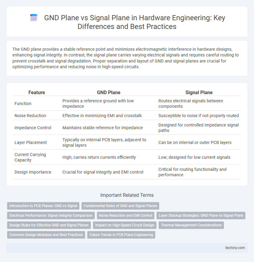
Table of Comparison
| Feature | GND Plane | Signal Plane |
|---|---|---|
| Function | Provides a reference ground with low impedance | Routes electrical signals between components |
| Noise Reduction | Effective in minimizing EMI and crosstalk | Susceptible to noise if not properly routed |
| Impedance Control | Maintains stable reference for impedance | Designed for controlled impedance signal paths |
| Layer Placement | Typically on internal PCB layers, adjacent to signal layers | Can be on internal or outer PCB layers |
| Current Carrying Capacity | High; carries return currents efficiently | Low; designed for low current signals |
| Design Importance | Crucial for signal integrity and EMI control | Critical for routing functionality and performance |
Introduction to PCB Planes: GND vs Signal
PCB planes serve distinct functions in hardware engineering; the GND plane provides a reference voltage and minimizes electromagnetic interference by offering a low-impedance path for return currents. Signal planes route electrical signals between components while maintaining controlled impedance and minimizing crosstalk. Understanding the interplay of GND and signal planes is crucial for optimizing signal integrity and overall circuit performance in PCB design.
Fundamental Roles of GND and Signal Planes
The GND plane serves as a stable reference voltage and provides a low-impedance return path for current, minimizing electromagnetic interference and maintaining signal integrity. The signal plane carries the actual data or power signals and requires careful layout to reduce crosstalk and signal degradation. Effective separation and design of GND and signal planes are essential for ensuring optimal electrical performance and system reliability in hardware engineering.
Electrical Performance: Signal Integrity Comparison
A dedicated GND plane in hardware engineering significantly enhances signal integrity by providing a low-inductance return path for signals, reducing electromagnetic interference and minimizing crosstalk. In contrast, a signal plane carries high-speed signals but lacks the consistent reference needed to maintain signal quality, often resulting in increased noise and signal distortion. Optimizing PCB stack-up with a continuous GND plane adjacent to signal layers ensures better impedance control, cleaner signal transitions, and improved overall electrical performance.
Noise Reduction and EMI Control
A well-designed GND plane provides a low-impedance path that significantly reduces noise by stabilizing reference voltages and minimizing ground loops. Signal planes must be carefully arranged to avoid coupling and crosstalk, which can increase electromagnetic interference (EMI) and degrade signal integrity. Proper separation and layering between GND and signal planes enhance noise reduction and EMI control, ensuring optimal hardware performance.
Layer Stackup Strategies: GND Plane vs Signal Plane
A well-designed layer stackup includes a dedicated GND plane to provide a low-impedance return path and minimize electromagnetic interference (EMI), improving overall signal integrity. Signal planes should be adjacent to GND planes to reduce loop inductance and crosstalk by tightly coupling the return currents. Strategic placement of GND and signal layers in multilayer PCB stackups enhances power distribution network performance and reduces noise in high-speed hardware engineering applications.
Design Rules for Effective GND and Signal Planes
Effective design rules for GND and signal planes emphasize maintaining low impedance paths by ensuring continuous, uninterrupted GND planes to minimize noise and EMI. Signal planes should be carefully routed with controlled impedance and proper spacing from GND planes to reduce crosstalk and signal reflection. Adhering to stack-up configurations with adjacent GND and signal layers enhances signal integrity and electromagnetic compatibility.
Impact on High-Speed Circuit Design
The GND plane provides a low-inductance return path, significantly reducing electromagnetic interference (EMI) and maintaining signal integrity in high-speed circuit design. Signal planes must be carefully routed to minimize crosstalk and impedance discontinuities, which can cause signal reflections and timing errors at gigahertz frequencies. Proper separation and controlled impedance between GND and signal planes are essential for achieving optimal performance in high-speed PCB layouts.
Thermal Management Considerations
GND planes provide superior thermal dissipation due to their continuous copper area, effectively spreading heat generated by components and minimizing hot spots in hardware designs. Signal planes, composed of narrower traces, offer limited thermal conductivity and can cause localized temperature rises, impacting signal integrity and component reliability. Integrating a solid GND plane adjacent to heat-generating components optimizes thermal management and enhances overall system stability in PCB layouts.
Common Design Mistakes and Best Practices
In hardware engineering, common design mistakes with GND planes include fragmentation and inadequate grounding, which can lead to signal integrity issues and increased electromagnetic interference (EMI). Best practices emphasize maintaining a continuous, unbroken GND plane to provide a low-impedance return path and minimize noise coupling. Signal planes should be routed over a solid GND plane with controlled impedance, avoiding splits and vias that disrupt current flow and degrade overall performance.
Future Trends in PCB Plane Engineering
Future trends in PCB plane engineering highlight the increasing integration of advanced GND planes to minimize electromagnetic interference and improve signal integrity in high-speed circuits. Innovations include multi-layer GND planes with optimized impedance control and adaptive segmentation techniques for enhanced noise reduction. Signal planes are evolving with dynamic routing algorithms and embedded components to support higher data rates and flexible design architectures.
GND plane vs Signal plane Infographic