The power plane in hardware engineering serves as a dedicated layer for distributing power and ground across the PCB, ensuring stable voltage levels and reducing noise. The signal plane, on the other hand, carries the data and control signals, requiring careful impedance control and isolation to maintain signal integrity. Proper separation and design of power and signal planes minimize electromagnetic interference and enhance overall device performance.
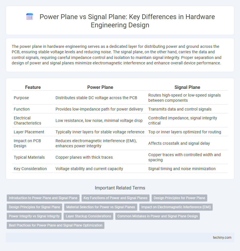
Table of Comparison
| Feature | Power Plane | Signal Plane |
|---|---|---|
| Purpose | Distributes stable DC voltage across the PCB | Routes high-speed or low-speed signals between components |
| Function | Provides low-impedance path for power delivery | Transmits data and control signals |
| Electrical Characteristics | Low resistance, low noise, minimal voltage drop | Controlled impedance, signal integrity critical |
| Layer Placement | Typically inner layers for stable voltage reference | Top or inner layers optimized for routing |
| Impact on PCB Design | Reduces electromagnetic interference (EMI), enhances power integrity | Affects crosstalk and signal delay |
| Typical Materials | Copper planes with thick traces | Copper traces with controlled width and spacing |
| Key Consideration | Voltage stability and current capacity | Signal timing and noise minimization |
Introduction to Power Plane and Signal Plane
Power planes in hardware engineering serve as dedicated layers within a printed circuit board (PCB) designed to distribute stable voltage and current efficiently to various components, minimizing noise and voltage drop. Signal planes, on the other hand, are layers allocated for routing high-speed data and control signals, optimized to reduce crosstalk and maintain signal integrity. Understanding the distinction between power and signal planes is crucial for effective PCB layout, ensuring reliable power delivery and optimal communication between integrated circuits.
Key Functions of Power and Signal Planes
Power planes provide stable voltage distribution and minimize electrical noise by delivering consistent current to components across the PCB, enhancing overall power integrity. Signal planes facilitate controlled impedance and reduce crosstalk by offering dedicated pathways for signal transmission, ensuring high-speed data integrity and reliable communication. Effective segregation of power and signal planes optimizes electromagnetic compatibility and improves the performance of complex hardware systems.
Design Principles for Power Plane
Power plane design principles prioritize low impedance and robust current distribution to ensure stable voltage levels and minimize electromagnetic interference (EMI). Utilizing continuous, uninterrupted copper areas with minimal splits enhances power integrity and thermal dissipation efficiency. Proper decoupling capacitor placement adjacent to power planes further reduces voltage fluctuations, critical for high-speed hardware performance.
Design Principles for Signal Plane
Signal plane design principles prioritize minimizing noise and crosstalk by maintaining consistent impedance and proper layer stacking. It is essential to route high-speed signals away from power planes to reduce electromagnetic interference and ensure signal integrity. Using controlled impedance traces and adequate spacing further enhances performance in complex hardware systems.
Material Selection for Power vs Signal Planes
Material selection for power planes prioritizes low resistivity and high thermal conductivity metals like copper to ensure efficient current distribution and heat dissipation. Signal planes require materials with controlled dielectric constants and low loss tangents to maintain signal integrity and minimize electromagnetic interference. Dielectric substrates such as FR-4 or high-frequency laminates are chosen based on the frequency and performance criteria of the signal paths.
Impact on Electromagnetic Interference (EMI)
Power planes provide a low-impedance return path that significantly reduces electromagnetic interference (EMI) by minimizing loop areas and stabilizing voltage levels. Signal planes, if poorly referenced or segmented, can increase EMI due to disrupted return currents and higher loop inductance. Proper stack-up design placing power and signal planes in close proximity helps to contain EMI within PCB layers, improving overall electromagnetic compatibility.
Power Integrity vs Signal Integrity
Power planes maintain a stable voltage level and minimize noise by providing low impedance paths for power delivery, which is critical for power integrity in hardware engineering. Signal planes ensure clean signal transmission by reducing crosstalk and electromagnetic interference, thereby preserving signal integrity. Optimal PCB design balances power plane placement and signal plane routing to enhance overall system performance and reliability.
Layer Stackup Considerations
In hardware engineering, power plane and signal plane layer stackup requires meticulous attention to electromagnetics and noise reduction. Power planes distribute stable voltage across the PCB with low impedance, necessitating continuous, unbroken layers to minimize voltage drop and electromagnetic interference (EMI). Signal planes demand controlled impedance and strategic separation from power planes to reduce crosstalk, optimize signal integrity, and enhance overall system performance.
Common Mistakes in Power and Signal Plane Design
Common mistakes in power and signal plane design include improper separation of power and ground planes, which can lead to increased electromagnetic interference (EMI) and signal crosstalk. Failing to maintain adequate decoupling capacitor placement near integrated circuits reduces power integrity and causes voltage fluctuations. Inadequate plane impedance control and fragmented return current paths result in signal integrity issues and degraded overall hardware performance.
Best Practices for Power Plane and Signal Plane Optimization
Optimal power plane design involves maintaining low impedance by using continuous, unbroken copper layers with minimal split planes to reduce voltage fluctuations and electromagnetic interference (EMI). Signal plane optimization requires carefully routing high-speed signals with controlled impedance, avoiding right-angle bends, and maintaining proper spacing from the power planes to minimize crosstalk and signal integrity issues. Employing simultaneous switching noise (SSN) mitigation techniques such as stitching capacitors and strategically placed decoupling capacitors further enhances overall PCB performance.
Power Plane vs Signal Plane Infographic