Electromigration occurs when high current density causes metal atoms in interconnects to migrate, leading to circuit failures such as open or short circuits. Dielectric breakdown happens when the insulating material between conductors loses its insulating properties under high electric fields, resulting in permanent damage and leakage paths. Understanding the distinct mechanisms and effects of electromigration versus dielectric breakdown is crucial for designing reliable integrated circuits and improving hardware longevity.
Table of Comparison
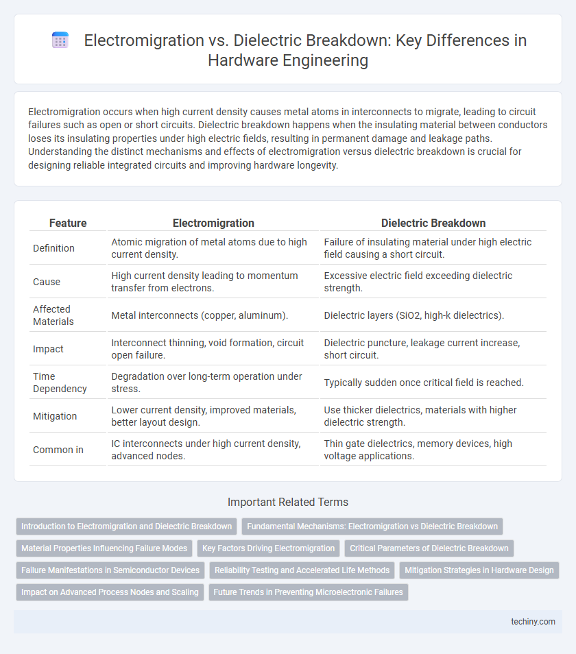
| Feature | Electromigration | Dielectric Breakdown |
|---|---|---|
| Definition | Atomic migration of metal atoms due to high current density. | Failure of insulating material under high electric field causing a short circuit. |
| Cause | High current density leading to momentum transfer from electrons. | Excessive electric field exceeding dielectric strength. |
| Affected Materials | Metal interconnects (copper, aluminum). | Dielectric layers (SiO2, high-k dielectrics). |
| Impact | Interconnect thinning, void formation, circuit open failure. | Dielectric puncture, leakage current increase, short circuit. |
| Time Dependency | Degradation over long-term operation under stress. | Typically sudden once critical field is reached. |
| Mitigation | Lower current density, improved materials, better layout design. | Use thicker dielectrics, materials with higher dielectric strength. |
| Common in | IC interconnects under high current density, advanced nodes. | Thin gate dielectrics, memory devices, high voltage applications. |
Introduction to Electromigration and Dielectric Breakdown
Electromigration is the gradual displacement of metal atoms in a conductor caused by high current density, leading to circuit failure in semiconductor devices. Dielectric breakdown occurs when an insulating material experiences a critical electric field, causing a sudden surge of current and permanent damage to the dielectric layer. Both phenomena are critical reliability concerns in hardware engineering, affecting the performance and durability of integrated circuits.
Fundamental Mechanisms: Electromigration vs Dielectric Breakdown
Electromigration is the transport of metal atoms caused by high-density electron flow, leading to voids and hillocks in interconnects, primarily driven by momentum transfer between conducting electrons and metal ions. Dielectric breakdown occurs when the insulating material within a semiconductor device fails due to excessive electric field stress, resulting in irreversible damage through mechanisms such as avalanche ionization and trap-assisted tunneling. Both phenomena limit device reliability, with electromigration predominantly affecting metal interconnect integrity and dielectric breakdown compromising insulating layers.
Material Properties Influencing Failure Modes
Electromigration primarily depends on metal conductivity and atomic diffusion rates within interconnect materials, where high current densities accelerate atom migration leading to void formation. Dielectric breakdown is influenced by the dielectric constant, breakdown strength, and defect density of insulating materials, resulting in catastrophic failure when electric fields exceed material limits. Material purity, grain structure, and thermal stability critically determine susceptibility to either failure mechanism in hardware engineering.
Key Factors Driving Electromigration
Electromigration in hardware engineering is primarily driven by high current density, elevated temperature, and material properties such as atom mobility and grain boundary structure. The momentum transfer from conducting electrons causes metal atoms to diffuse, leading to void formation and eventual circuit failure. Unlike dielectric breakdown, which results from electric field-induced insulation failure, electromigration is critically influenced by prolonged electrical stress and thermal gradients within interconnects.
Critical Parameters of Dielectric Breakdown
Dielectric breakdown in hardware engineering is primarily influenced by critical parameters such as the electric field strength, temperature, and material thickness, which determine the integrity of insulating layers in semiconductor devices. Electromigration, contrastingly, involves the movement of metal ions under high current density, affecting interconnect reliability rather than insulation integrity. Understanding the critical electric field threshold and thermal conditions is essential for preventing dielectric failure and ensuring long-term device performance.
Failure Manifestations in Semiconductor Devices
Electromigration causes metal interconnects in semiconductor devices to fail by the gradual movement of metal atoms under high current density, leading to voids and hillocks that disrupt electrical continuity. Dielectric breakdown occurs when the insulating layer within devices fails due to excessive electric fields, resulting in permanent short circuits or increased leakage currents. Both failure mechanisms degrade device reliability but manifest differently, with electromigration primarily affecting metal lines and dielectric breakdown compromising gate oxides or interlayer dielectrics.
Reliability Testing and Accelerated Life Methods
Reliability testing in hardware engineering differentiates electromigration and dielectric breakdown by applying accelerated life methods such as high-temperature storage and voltage stress tests to simulate prolonged operational conditions. Electromigration testing emphasizes current density and temperature-induced metal migration, while dielectric breakdown focuses on electrical field stress compromising insulator integrity. Advanced techniques like time-dependent dielectric breakdown (TDDB) and electromigration activation energy analysis enable precise lifetime prediction and failure mode identification in integrated circuits.
Mitigation Strategies in Hardware Design
Mitigation strategies for electromigration in hardware design include optimizing metal interconnect geometry, implementing lower current densities, and using barrier layers to prevent atomic migration. Dielectric breakdown prevention relies on selecting high-quality insulating materials, controlling electric field strengths, and employing advanced thin-film deposition techniques to improve dielectric robustness. Both failures demand comprehensive reliability testing and thermal management to enhance the longevity of semiconductor devices.
Impact on Advanced Process Nodes and Scaling
Electromigration and dielectric breakdown critically impact the reliability of advanced process nodes by accelerating failure mechanisms in densely packed interconnects and thin dielectric layers. Electromigration causes metal atom migration under high current density, leading to open circuits, while dielectric breakdown results from high electric fields degrading insulating materials, causing shorts. As feature sizes shrink below 7nm, scaling challenges intensify due to increased current densities and reduced dielectric thickness, necessitating new materials and process innovations to mitigate these failure modes.
Future Trends in Preventing Microelectronic Failures
Future trends in preventing microelectronic failures emphasize advanced materials and nanoscale design to mitigate electromigration and dielectric breakdown. Innovations in barrier metals, low-k dielectrics, and thermal management techniques enhance device reliability by reducing electron wind force and electric field stress. Machine learning algorithms predict failure modes, optimizing manufacturing processes and accelerating the development of resilient integrated circuits.
Electromigration vs Dielectric Breakdown Infographic