Miller Effect describes the apparent increase in input capacitance due to feedback through an amplification stage, significantly impacting high-frequency response in hardware engineering. Miller Capacitance refers specifically to the capacitance between the input and output terminals of a transistor or amplifier, which is the primary cause of the Miller Effect. Understanding the distinction between Miller Effect and Miller Capacitance is crucial for optimizing circuit designs and minimizing signal distortion in high-speed electronic devices.
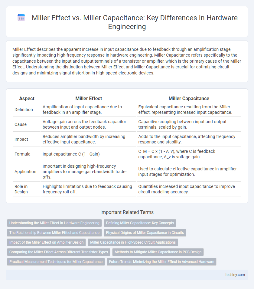
Table of Comparison
| Aspect | Miller Effect | Miller Capacitance |
|---|---|---|
| Definition | Amplification of input capacitance due to feedback in an amplifier stage. | Equivalent capacitance resulting from the Miller effect, representing increased input capacitance. |
| Cause | Voltage gain across the feedback capacitor between input and output nodes. | Capacitive coupling between input and output terminals, scaled by gain. |
| Impact | Reduces amplifier bandwidth by increasing effective input capacitance. | Adds to the input capacitance, affecting frequency response and stability. |
| Formula | Input capacitance C (1 - Gain) | C_M = C x (1 - A_v), where C is feedback capacitance, A_v is voltage gain. |
| Application | Important in designing high-frequency amplifiers to manage gain-bandwidth trade-offs. | Used to calculate effective capacitance in amplifier input stages for optimization. |
| Role in Design | Highlights limitations due to feedback causing frequency roll-off. | Quantifies increased input capacitance to improve circuit modeling accuracy. |
Understanding the Miller Effect in Hardware Engineering
The Miller Effect describes the amplification of the input capacitance due to feedback through an inverting gain stage, significantly impacting high-frequency performance in hardware engineering. Miller Capacitance specifically refers to the equivalent input capacitance increased by this effect, often modeled as a multiplied capacitance value that influences the bandwidth and stability of amplifiers. Engineers must consider the Miller Effect when designing circuits to accurately predict gain and frequency response, optimizing overall system performance.
Defining Miller Capacitance: Key Concepts
Miller capacitance refers to the effective increase in input capacitance of an amplifier stage caused by the feedback through a gain stage, typically modeled as the product of the amplifier's gain and the inherent parasitic capacitance between input and output nodes. This phenomenon significantly impacts high-frequency performance by amplifying the input capacitance, thereby reducing bandwidth and slowing response times in hardware circuits. Understanding Miller capacitance is essential for optimizing amplifier design, improving signal integrity, and mitigating unwanted frequency roll-off in analog hardware engineering.
The Relationship Between Miller Effect and Capacitance
Miller Effect describes the amplification of an input capacitance due to feedback through a gain stage, significantly increasing the effective input capacitance known as Miller capacitance. Miller capacitance is the apparent capacitance seen at the input, calculated as the original capacitance multiplied by the gain factor minus one, impacting high-frequency response in amplifier circuits. Understanding the relationship between Miller Effect and Miller capacitance is essential for accurate modeling of frequency behavior and optimizing bandwidth in hardware engineering applications.
Physical Origins of Miller Capacitance in Circuits
Miller capacitance originates from the feedback capacitance between the input and output terminals of an amplifier, caused by the intrinsic parasitic capacitances within transistor junctions. This capacitance is physically manifested due to the coupling of the gate-to-drain or base-to-collector capacitances that get multiplied by the gain of the circuit. The Miller effect describes how this intrinsic capacitor presents an amplified input capacitance, significantly impacting the frequency response and bandwidth of high-gain amplifiers in hardware design.
Impact of the Miller Effect on Amplifier Design
The Miller Effect significantly influences amplifier design by effectively increasing the input capacitance through feedback capacitance multiplication, which can reduce bandwidth and slow frequency response. This phenomenon arises due to the Miller Capacitance, the equivalent capacitance seen at the input resulting from amplification of the feedback capacitance between input and output nodes. Engineers must account for the Miller Effect to optimize gain-bandwidth product and ensure stable, high-speed amplifier performance in integrated circuits.
Miller Capacitance in High-Speed Circuit Applications
Miller capacitance, an inherent parasitic capacitance between the input and output terminals of an amplifier, significantly impacts bandwidth and phase margin in high-speed circuit applications. Its amplification effect due to circuit gain increases the effective input capacitance, thereby limiting the frequency response and causing signal distortion. Effective mitigation techniques involve circuit design strategies such as neutralization, cascode configurations, and careful selection of transistor parameters to enhance high-frequency performance.
Comparing the Miller Effect Across Different Transistor Types
The Miller effect varies significantly across bipolar junction transistors (BJTs), metal-oxide-semiconductor field-effect transistors (MOSFETs), and junction field-effect transistors (JFETs) due to differences in their intrinsic capacitances and input impedances. BJTs exhibit a pronounced Miller capacitance as a result of the amplified virtual capacitance at the base-collector junction, while MOSFETs demonstrate a more complex Miller effect influenced by gate-to-drain overlap capacitance and channel modulation. JFETs typically show a reduced Miller effect because of their depletion-mode operation and smaller gate-to-channel capacitance, making the choice of transistor critical in high-frequency analog circuit design.
Methods to Mitigate Miller Capacitance in PCB Design
Miller capacitance, a parasitic effect caused by the amplified input-to-output capacitance in amplifiers, can degrade high-frequency performance in PCB designs. Techniques to mitigate Miller capacitance include employing cascode amplifier configurations, which reduce voltage gain across the parasitic capacitor, and using neutralization circuits to cancel out the Miller effect. Additionally, optimizing PCB layout by minimizing trace lengths and implementing proper grounding helps reduce parasitic capacitances and improves signal integrity.
Practical Measurement Techniques for Miller Capacitance
Miller capacitance is an intrinsic parasitic capacitance in amplifying devices, significantly affecting high-frequency performance and stability. Practical measurement techniques involve using impedance analyzers or network analyzers with test circuits configured to isolate the feedback capacitance by carefully calibrating input and output impedances. Accurate extraction often requires the implementation of nulling methods or the use of equivalent circuit models to separate Miller capacitance from overlap and parasitic capacitances.
Future Trends: Minimizing the Miller Effect in Advanced Hardware
Emerging hardware engineering trends emphasize advanced circuit design techniques and novel transistor architectures to minimize the Miller effect, thereby reducing the Miller capacitance that limits high-frequency performance. Techniques such as neutralization circuits, cascode configurations, and the integration of nanomaterials enable significant suppression of parasitic capacitances, enhancing signal integrity and switching speeds in next-generation devices. These innovations are critical for innovations in RF amplifiers, high-speed ADCs, and low-power integrated circuits aiming to overcome traditional Miller effect constraints.
Miller Effect vs Miller Capacitance Infographic