Clock gating reduces dynamic power consumption by disabling the clock signal to inactive modules, effectively preventing unnecessary switching activity. Power gating, on the other hand, shuts off the power supply to idle circuits, eliminating both dynamic and leakage power but requiring state retention strategies for quick wake-up. Both techniques optimize power efficiency in hardware design, with clock gating offering finer control and power gating delivering more substantial savings during longer idle periods.
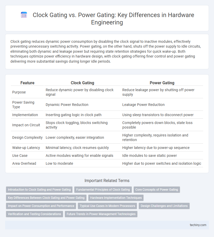
Table of Comparison
| Feature | Clock Gating | Power Gating |
|---|---|---|
| Purpose | Reduce dynamic power by disabling clock signal | Reduce leakage power by shutting off power supply |
| Power Saving Type | Dynamic Power Reduction | Leakage Power Reduction |
| Implementation | Inserting gating logic in clock path | Using sleep transistors to disconnect power |
| Impact on Circuit | Stops clock toggling, blocks switching activity | Completely powers down blocks, state loss possible |
| Design Complexity | Lower complexity, easier integration | Higher complexity, requires isolation and retention |
| Wake-up Latency | Minimal latency, clock resumes quickly | Higher latency due to power-up sequence |
| Use Case | Active modules waiting for enable signals | Idle modules to save static power |
| Area Overhead | Low to moderate | Higher due to power switches and isolation logic |
Introduction to Clock Gating and Power Gating
Clock gating reduces dynamic power consumption by disabling the clock signal to inactive modules, effectively minimizing switching activity within a digital circuit. Power gating conserves leakage power by completely cutting off the power supply to idle blocks using sleep transistors, thereby reducing static current flow. Both techniques are essential for optimizing power efficiency in modern hardware designs, with clock gating targeting dynamic power and power gating focusing on static power reduction.
Fundamental Principles of Clock Gating
Clock gating fundamentally reduces dynamic power consumption by selectively disabling the clock signal to inactive modules, preventing unnecessary switching activities in flip-flops and sequential logic. It operates by integrating gating logic into the clock distribution network, enabling fine-grained control over clock pulses based on circuit activity. This technique contrasts with power gating, which focuses on cutting off power supply to idle blocks to minimize static leakage current, emphasizing the unique approach of clock gating on controlling timing signals rather than voltage domains.
Core Concepts of Power Gating
Power gating is a technique used in hardware engineering to reduce leakage power by shutting off the power supply to idle circuit blocks, effectively isolating them from the power grid. This approach contrasts with clock gating, which only disables the clock signal to a circuit to reduce dynamic power while keeping the circuit powered. Core concepts of power gating involve the use of sleep transistors that create a power island, enabling significant power savings during idle periods by completely cutting off supply voltage and thereby minimizing static power consumption.
Key Differences Between Clock Gating and Power Gating
Clock gating reduces dynamic power consumption by disabling the clock signal to inactive circuits, effectively stopping switching activity without cutting power supply, preserving circuit state. Power gating saves leakage power by completely shutting off the power supply to idle blocks using sleep transistors, resulting in loss of data state and requiring wake-up latency. Key differences include their impact on power domains: clock gating controls clock distribution within an always-powered domain, while power gating isolates entire power domains to minimize leakage power during inactivity.
Hardware Implementation Techniques
Clock gating reduces dynamic power consumption by selectively disabling the clock signal to idle circuit blocks using AND or OR logic gates integrated into the clock distribution network. Power gating cuts leakage power by inserting sleep transistors, typically header or footer transistors, to disconnect the power supply from inactive circuit sections, effectively reducing static current. Hardware implementation of clock gating demands precise timing control and logic synthesis integration, while power gating requires careful design of power switch sizing and retention strategies to maintain state during power-down modes.
Impact on Power Consumption and Performance
Clock gating reduces dynamic power consumption by disabling the clock signal to inactive circuitry, minimizing unnecessary switching activity without affecting the logic state, thus maintaining system performance. Power gating significantly lowers leakage power by cutting off the power supply to idle blocks, but it incurs a wake-up latency that can impact performance due to the need to restore power and state. Optimizing the balance between clock gating and power gating enables hardware engineers to achieve efficient power management while minimizing performance degradation in integrated circuits.
Typical Use Cases in Modern Processors
Clock gating is typically used in modern processors to reduce dynamic power by disabling the clock signal in inactive modules, making it ideal for fine-grained power management in sequential logic circuits. Power gating, on the other hand, effectively reduces leakage power by completely shutting off the power supply to idle blocks, which is crucial for low-power states and extended battery life in mobile and embedded processors. Combining clock gating with power gating enables processors to optimize power savings across different operational states without compromising performance.
Design Challenges and Limitations
Clock gating reduces dynamic power consumption by disabling the clock signal to inactive modules but faces challenges in maintaining signal integrity and timing accuracy during gating insertion. Power gating effectively minimizes leakage power by cutting off the power supply to idle blocks, yet it introduces complexity in state retention and wake-up latency management. Both techniques require careful design trade-offs to balance power savings with performance impact and increased area overhead.
Verification and Testing Considerations
Clock gating reduces dynamic power by disabling the clock signal to idle circuits, requiring verification to focus on clock domain crossing issues and glitch-free timing analysis. Power gating cuts leakage power by shutting off the power supply to unused blocks, necessitating thorough testing of power switch functionality, state retention, and wake-up sequences to prevent data corruption. Both techniques demand comprehensive formal and functional verification to ensure correct operation under all power management modes.
Future Trends in Power Management Technologies
Future trends in power management technologies emphasize integrating advanced clock gating with dynamic power gating techniques to achieve ultra-low power consumption in hardware engineering. Emerging methodologies leverage fine-grained clock gating alongside adaptive power gating to optimize energy efficiency in complex integrated circuits. Innovations in Machine Learning-driven control units enable predictive gating strategies, enhancing power savings while maintaining system performance in next-generation semiconductor devices.
Clock gating vs Power gating Infographic