PCB traces offer precise, compact routing for signals and power, ensuring minimal interference and reliable performance in hardware engineering designs. Wire jumpers provide flexibility for quick modifications and repairs but introduce higher inductance and potential signal integrity issues, making them less ideal for high-frequency circuits. Careful consideration of signal requirements and circuit complexity determines the optimal choice between PCB traces and wire jumpers.
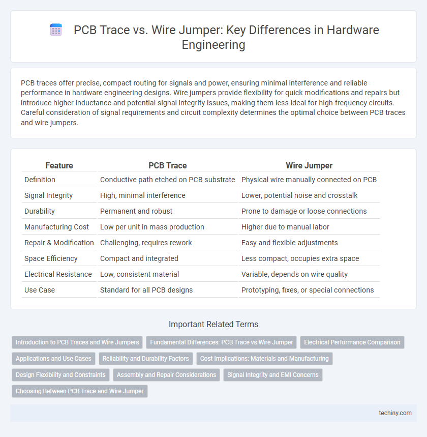
Table of Comparison
| Feature | PCB Trace | Wire Jumper |
|---|---|---|
| Definition | Conductive path etched on PCB substrate | Physical wire manually connected on PCB |
| Signal Integrity | High, minimal interference | Lower, potential noise and crosstalk |
| Durability | Permanent and robust | Prone to damage or loose connections |
| Manufacturing Cost | Low per unit in mass production | Higher due to manual labor |
| Repair & Modification | Challenging, requires rework | Easy and flexible adjustments |
| Space Efficiency | Compact and integrated | Less compact, occupies extra space |
| Electrical Resistance | Low, consistent material | Variable, depends on wire quality |
| Use Case | Standard for all PCB designs | Prototyping, fixes, or special connections |
Introduction to PCB Traces and Wire Jumpers
PCB traces are thin conductive pathways etched on a printed circuit board, designed to efficiently route electrical signals between components with minimal interference and signal loss. Wire jumpers serve as manual connections or repairs, bridging non-continuous traces or bypassing damaged sections to maintain circuit integrity. Understanding the electrical characteristics and physical layout differences between PCB traces and wire jumpers is essential for optimizing circuit performance and reliability in hardware engineering.
Fundamental Differences: PCB Trace vs Wire Jumper
PCB traces are thin conductive pathways etched directly onto the board's substrate, providing fixed, low-resistance connections essential for high-speed signal integrity and compact circuit layout. Wire jumpers are insulated, manually placed wires used to bridge PCB traces or correct design errors, offering flexibility but introducing higher inductance and potential signal interference. The fundamental difference lies in permanence and electrical performance: PCB traces ensure reliable, repeatable connections with minimal parasitic effects, while wire jumpers serve as temporary or corrective solutions with comparatively degraded electrical characteristics.
Electrical Performance Comparison
PCB traces typically offer lower inductance and capacitance compared to wire jumpers, resulting in enhanced signal integrity and reduced electromagnetic interference (EMI). Wire jumpers introduce additional parasitic elements such as increased resistance and susceptibility to noise, which can degrade high-frequency signal transmission. For high-speed or high-frequency circuits, optimized PCB trace design is preferable to maintain electrical performance and minimize signal loss.
Applications and Use Cases
PCB traces are preferred in high-frequency and high-density circuit designs due to their low inductance and precise impedance control, making them ideal for automated manufacturing and compact layouts. Wire jumpers are commonly used for prototyping, repairs, or modifications where quick changes are required, offering flexibility to bypass or connect specific nodes on the PCB. In applications demanding signal integrity and reliability, such as RF circuits, traces are favored, while wire jumpers excel in troubleshooting and iterative design processes.
Reliability and Durability Factors
PCB traces offer superior reliability and durability compared to wire jumpers due to their consistent manufacturing process and controlled impedance, which minimizes signal degradation and mechanical failure. Wire jumpers are prone to oxidation, physical damage, and connection instability over time, especially in environments with vibration or thermal cycling. Properly designed and fabricated PCB traces ensure long-term electrical performance and robustness in complex hardware engineering applications.
Cost Implications: Materials and Manufacturing
PCB traces offer a cost-effective solution by reducing material usage and simplifying manufacturing processes compared to wire jumpers. Wire jumpers require additional conductive materials and manual labor, increasing both material costs and assembly time. Optimizing PCB trace design minimizes overall production expenses while enhancing reliability in hardware engineering projects.
Design Flexibility and Constraints
PCB traces offer precise routing with compact, consistent impedance control, enhancing signal integrity in high-density circuit layouts. Wire jumpers provide adaptable bypass options for design modifications or error corrections, especially useful during prototyping or late-stage revisions. However, traces are constrained by fixed PCB layers and etching precision, while wire jumpers introduce potential electromagnetic interference and increased assembly complexity.
Assembly and Repair Considerations
PCB trace offers streamlined assembly with automated manufacturing processes, reducing human error and improving production consistency. Wire jumpers facilitate quick, manual repairs or design modifications on populated boards, enabling targeted fixes without full PCB replacement. Selecting between PCB trace and wire jumper depends on balancing initial assembly efficiency against ease of post-production troubleshooting and repair.
Signal Integrity and EMI Concerns
PCB traces provide controlled impedance and consistent geometry, which enhances signal integrity by minimizing reflections and crosstalk compared to wire jumpers. Wire jumpers introduce parasitic inductance and unpredictable impedance, increasing susceptibility to electromagnetic interference (EMI) and degrading high-frequency signal quality. Careful PCB trace design with proper grounding and shielding is essential to mitigate EMI and maintain optimal signal performance in hardware engineering applications.
Choosing Between PCB Trace and Wire Jumper
Selecting between PCB trace and wire jumper depends on factors like signal integrity, space constraints, and manufacturing complexity. PCB traces offer better reliability, compactness, and reduced parasitic inductance, making them ideal for high-frequency applications and automated production. Wire jumpers provide flexibility for prototyping or correcting design errors but increase manual labor and potential signal interference.
PCB Trace vs Wire Jumper Infographic