Blind vias connect outer layers to one or more inner layers without passing through the entire printed circuit board, optimizing space and signal integrity in high-density designs. Buried vias, in contrast, exist exclusively between inner layers and remain hidden within the PCB, providing enhanced routing flexibility while preserving surface layer real estate. Choosing between blind and buried vias depends on factors like electrical performance requirements, manufacturing complexity, and cost constraints.
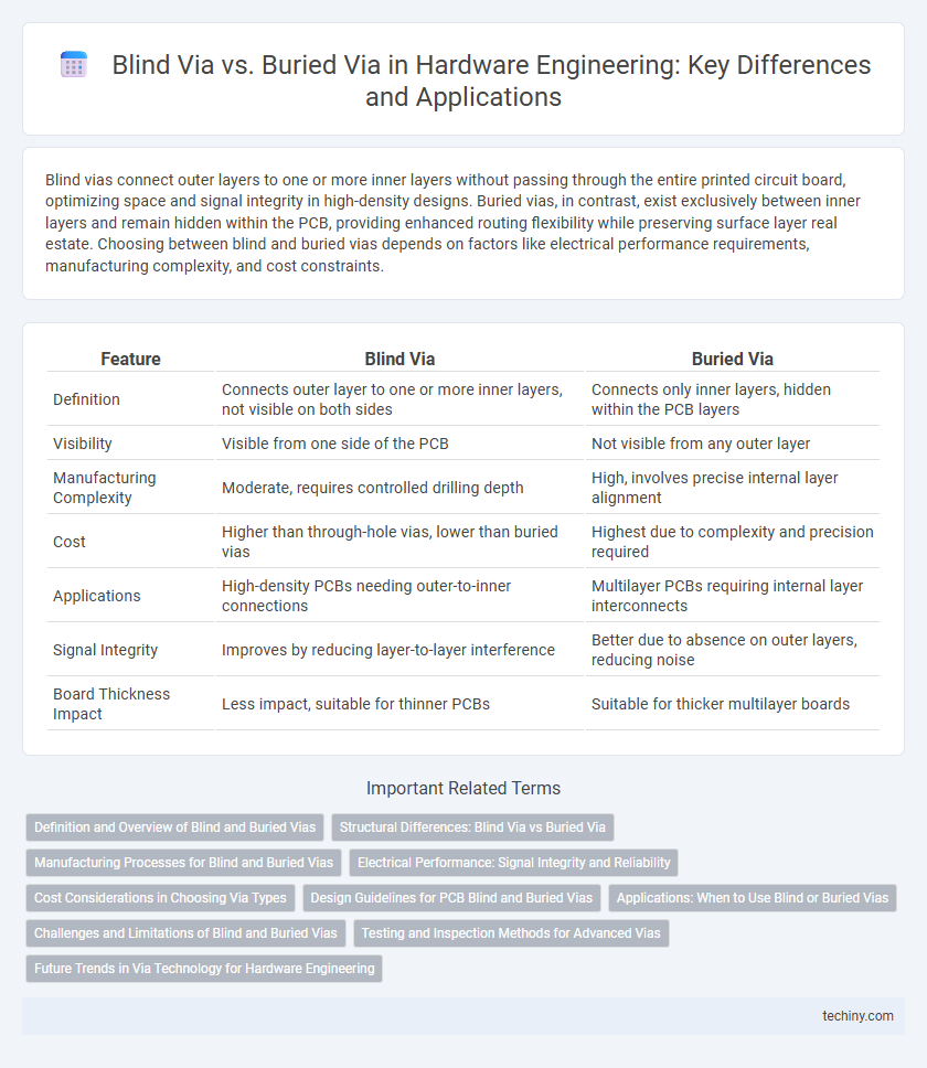
Table of Comparison
| Feature | Blind Via | Buried Via |
|---|---|---|
| Definition | Connects outer layer to one or more inner layers, not visible on both sides | Connects only inner layers, hidden within the PCB layers |
| Visibility | Visible from one side of the PCB | Not visible from any outer layer |
| Manufacturing Complexity | Moderate, requires controlled drilling depth | High, involves precise internal layer alignment |
| Cost | Higher than through-hole vias, lower than buried vias | Highest due to complexity and precision required |
| Applications | High-density PCBs needing outer-to-inner connections | Multilayer PCBs requiring internal layer interconnects |
| Signal Integrity | Improves by reducing layer-to-layer interference | Better due to absence on outer layers, reducing noise |
| Board Thickness Impact | Less impact, suitable for thinner PCBs | Suitable for thicker multilayer boards |
Definition and Overview of Blind and Buried Vias
Blind vias connect outer layers to one or more inner layers without penetrating the entire printed circuit board (PCB), optimizing space and signal integrity in high-density designs. Buried vias are confined entirely within inner layers, invisible from the outer surfaces, enabling complex multilayer PCB routing without affecting external layer real estate. Both via types enhance PCB functionality by facilitating dense interconnections while maintaining structural integrity and electrical performance.
Structural Differences: Blind Via vs Buried Via
Blind vias connect outer layers to one or more inner layers without passing through the entire printed circuit board, preserving surface area and reducing signal interference. Buried vias are embedded completely within inner layers, isolated from outer layers, enhancing circuit density and improving signal integrity in multilayer PCBs. The structural difference lies in blind vias being partially visible from the surface while buried vias remain entirely enclosed within the PCB core.
Manufacturing Processes for Blind and Buried Vias
Blind vias connect outer layers to one or more inner layers without penetrating the entire PCB, requiring precise laser drilling or mechanical drilling controlled by advanced computer numerical control (CNC) systems to ensure accuracy and reliability. Buried vias link only inner layers, demanding multilayer lamination processes where vias are drilled and plated before outer layers are added, emphasizing strict alignment and controlled thermal cycles to maintain structural integrity. Both manufacturing processes rely heavily on photolithography, electroless copper plating, and rigorous inspection techniques such as X-ray and automated optical inspection (AOI) to meet high-density interconnect (HDI) design specifications.
Electrical Performance: Signal Integrity and Reliability
Blind vias, which connect outer layers to one or more inner layers without passing through the entire PCB, offer improved signal integrity by minimizing parasitic capacitance and inductance compared to through-hole vias. Buried vias, embedded entirely within inner layers, further enhance electrical performance by reducing signal path lengths and crosstalk, crucial for high-speed circuit reliability. Both via types optimize grounding and reduce electromagnetic interference, thereby boosting overall signal quality and long-term manufacturing durability in multilayer PCB designs.
Cost Considerations in Choosing Via Types
Blind vias offer a cost-effective solution for multilayer PCBs by limiting drilling depth and reducing material usage, which lowers manufacturing expenses compared to through-hole vias. Buried vias, embedded entirely within inner layers, increase complexity and require more precise alignment, leading to higher fabrication costs. Choosing between blind and buried vias depends on balancing budget constraints with design requirements for signal integrity and layer interconnections.
Design Guidelines for PCB Blind and Buried Vias
Design guidelines for PCB blind and buried vias emphasize minimizing signal integrity issues by controlling via size, aspect ratio, and plating thickness. Blind vias connect outer layers to one or more inner layers without passing through the entire board, requiring precise drilling depths and careful thermal management to maintain reliability. Buried vias are located entirely within internal layers, demanding strict adherence to layer stack-up and lamination processes to ensure electrical performance and structural stability.
Applications: When to Use Blind or Buried Vias
Blind vias are ideal for high-density printed circuit boards (PCBs) where components require interconnections on outer layers without penetrating the entire board, optimizing space in compact designs like smartphones and laptops. Buried vias connect internal layers exclusively, enhancing signal integrity and reducing electromagnetic interference in multilayer PCBs used in advanced telecommunications and aerospace systems. Choosing between blind and buried vias depends on design complexity, layer count, and the need for minimizing board size while maintaining electrical performance in hardware engineering projects.
Challenges and Limitations of Blind and Buried Vias
Blind and buried vias present challenges such as increased manufacturing complexity and higher production costs due to precise layer alignment requirements in multi-layer PCBs. The limitations include restricted current-carrying capacity and potential reliability issues from thermal stress or mechanical fatigue during soldering or operation. Additionally, inspection and repair of these vias are more difficult compared to through-hole vias, complicating quality control processes.
Testing and Inspection Methods for Advanced Vias
Blind vias and buried vias in advanced hardware engineering require rigorous testing and inspection methods to ensure reliability and signal integrity. Techniques such as X-ray tomography and cross-sectional analysis enable non-destructive evaluation of via depth, alignment, and integrity, critical for identifying defects in multilayer PCB assemblies. Automated optical inspection (AOI) combined with electrical continuity testing enhances detection accuracy, ensuring optimal performance of complex via structures.
Future Trends in Via Technology for Hardware Engineering
Future trends in via technology for hardware engineering emphasize the increased integration of blind vias to enhance signal integrity and reduce board size in high-density PCBs. Advanced manufacturing techniques enable more precise buried vias, improving multilayer interconnections without compromising board reliability. Emerging materials and laser drilling technologies are expected to optimize via performance, supporting faster data transmission and enabling more compact, efficient electronic designs.
Blind via vs Buried via Infographic