Clock signals provide precise timing references essential for synchronizing data signals across hardware components, ensuring coordinated data transfers and operations. Data signals carry the actual information processed by circuits and rely on clock signals to establish valid sampling points to maintain data integrity. Differentiating between these signals is crucial in hardware design to optimize performance and prevent timing errors.
Table of Comparison
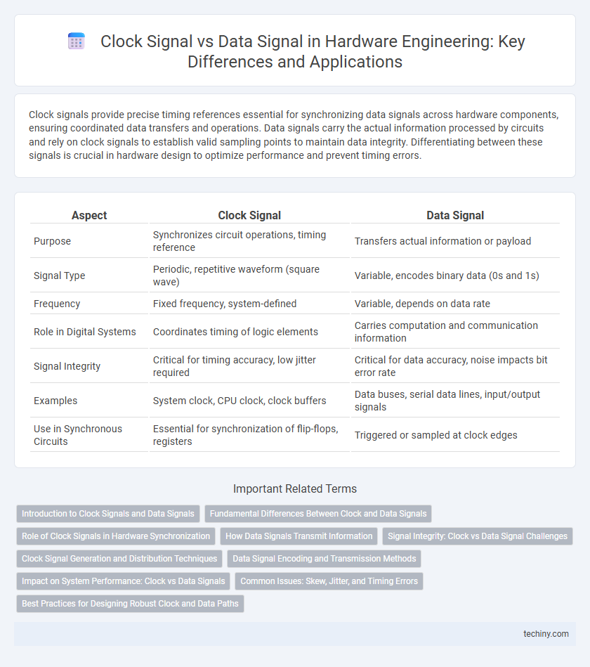
| Aspect | Clock Signal | Data Signal |
|---|---|---|
| Purpose | Synchronizes circuit operations, timing reference | Transfers actual information or payload |
| Signal Type | Periodic, repetitive waveform (square wave) | Variable, encodes binary data (0s and 1s) |
| Frequency | Fixed frequency, system-defined | Variable, depends on data rate |
| Role in Digital Systems | Coordinates timing of logic elements | Carries computation and communication information |
| Signal Integrity | Critical for timing accuracy, low jitter required | Critical for data accuracy, noise impacts bit error rate |
| Examples | System clock, CPU clock, clock buffers | Data buses, serial data lines, input/output signals |
| Use in Synchronous Circuits | Essential for synchronization of flip-flops, registers | Triggered or sampled at clock edges |
Introduction to Clock Signals and Data Signals
Clock signals serve as timing references that synchronize operations within digital circuits, ensuring data signals are sampled and processed at precise intervals. Data signals represent the actual binary information being transferred or manipulated, changing state according to the clock's timing to maintain system stability and accuracy. The interplay between clock and data signals is crucial for reliable hardware performance, enabling coordinated communication across components such as processors, memory units, and peripherals.
Fundamental Differences Between Clock and Data Signals
Clock signals provide a consistent timing reference used to synchronize the operations of digital circuits, characterized by their periodic, square waveform with a fixed frequency and duty cycle. Data signals, in contrast, carry variable information represented by voltage levels or pulses that change asynchronously and lack a fixed periodicity. The fundamental difference lies in the clock signal's role as a stable timing generator, while data signals serve as carriers of information that are interpreted based on the timing established by the clock.
Role of Clock Signals in Hardware Synchronization
Clock signals serve as a fundamental timing reference in hardware engineering, ensuring precise synchronization of data signals across digital circuits. They coordinate the sequential operation of flip-flops and registers by providing periodic pulses that dictate when data is sampled and transferred. Reliable clock distribution minimizes timing errors and enables coherent communication between various components within synchronous systems.
How Data Signals Transmit Information
Data signals transmit information by representing binary states through voltage levels that switch between high and low values, encoding digital bits as sequences of pulses. These signals synchronize with the clock signal to ensure accurate timing for data sampling and processing, maintaining the integrity and timing coherence essential in hardware communication. The precise alignment of data signals with clock edges allows hardware components to correctly interpret transmitted information without errors or data loss.
Signal Integrity: Clock vs Data Signal Challenges
Clock signals require strict timing accuracy and low jitter to maintain synchronization across hardware components, while data signals demand high signal integrity to ensure correct data interpretation amidst noise and crosstalk. The periodic nature of clock signals makes them vulnerable to phase noise and skew, impacting overall system performance. Data signals face challenges like inter-symbol interference and signal attenuation, necessitating advanced equalization and robust PCB layout strategies to preserve signal quality.
Clock Signal Generation and Distribution Techniques
Clock signal generation employs phase-locked loops (PLLs), crystal oscillators, and delay-locked loops (DLLs) to produce stable and precise timing references essential for synchronous circuits. Distribution techniques utilize balanced clock trees, H-tree topologies, and clock mesh networks to minimize skew and jitter, ensuring uniform clock arrival times across the chip. Advanced methods incorporate on-chip clock buffers and deskew circuits to optimize signal integrity and reduce latency in high-frequency hardware designs.
Data Signal Encoding and Transmission Methods
Data signal encoding and transmission methods are critical in hardware engineering to ensure accurate communication and timing synchronization. Techniques such as Non-Return to Zero (NRZ), Manchester encoding, and Pulse Amplitude Modulation (PAM) are employed to represent binary data efficiently over various channels. Proper encoding mitigates signal degradation, reduces electromagnetic interference, and optimizes bandwidth utilization in high-speed digital circuits.
Impact on System Performance: Clock vs Data Signals
Clock signals provide a stable timing reference essential for synchronizing data transfers, directly impacting the overall system performance by ensuring precise timing and minimizing latency. Data signals carry the actual information between components, and their integrity and timing alignment with the clock signal affect system throughput and error rates. Mismatches or jitter in clock signals can cause data signal errors, resulting in system inefficiencies and reduced performance.
Common Issues: Skew, Jitter, and Timing Errors
Clock signals and data signals in hardware engineering frequently encounter common issues such as skew, jitter, and timing errors that can significantly impact system performance. Skew arises from mismatched arrival times of signals at different components, causing synchronization problems. Jitter, defined as small deviations in signal timing, and timing errors, often due to setup and hold time violations, lead to data corruption and unreliable circuit operation.
Best Practices for Designing Robust Clock and Data Paths
Optimizing clock and data paths requires synchronizing clock signals with minimal skew to ensure timing accuracy and reduce setup and hold time violations. Employing differential signaling and impedance matching in data paths enhances signal integrity and minimizes noise interference. Careful layout planning, including short, matched-length routes for clock and data lines, prevents crosstalk and timing mismatches, leading to robust hardware designs.
clock signal vs data signal Infographic