Ground planes provide a stable reference voltage and help reduce electromagnetic interference by creating a continuous conductive surface, which enhances signal integrity. Signal planes, on the other hand, are dedicated layers for routing traces and signals, requiring careful layout to minimize crosstalk and signal distortion. Proper separation and alignment between ground planes and signal planes are critical in hardware engineering to optimize high-speed circuit performance and ensure reliable communication.
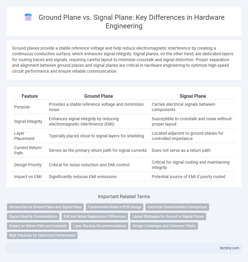
Table of Comparison
| Feature | Ground Plane | Signal Plane |
|---|---|---|
| Purpose | Provides a stable reference voltage and minimizes noise | Carries electrical signals between components |
| Signal Integrity | Enhances signal integrity by reducing electromagnetic interference (EMI) | Susceptible to crosstalk and noise without proper layout |
| Layer Placement | Typically placed close to signal layers for shielding | Located adjacent to ground planes for controlled impedance |
| Current Return Path | Serves as the primary return path for signal currents | Does not serve as a return path |
| Design Priority | Critical for noise reduction and EMI control | Critical for signal routing and maintaining integrity |
| Impact on EMI | Significantly reduces EMI emissions | Potential source of EMI if poorly routed |
Introduction to Ground Plane and Signal Plane
The ground plane in hardware engineering is a large conductor that serves as a reference point for all signals, providing a stable voltage level and minimizing electromagnetic interference (EMI). The signal plane is a layer within a printed circuit board (PCB) dedicated to routing electrical signals between components, optimized for signal integrity and controlled impedance. Proper design and placement of ground and signal planes are critical for ensuring reliable circuit performance and reduced noise coupling.
Fundamental Roles in PCB Design
A ground plane in PCB design serves as a stable reference point for electrical signals, reducing noise and electromagnetic interference by providing a low-impedance path for return currents. The signal plane carries high-speed data traces and must be closely coupled to the ground plane to maintain signal integrity and minimize crosstalk. Proper layout of ground and signal planes is essential for controlling impedance, improving signal quality, and ensuring reliable hardware performance in complex electronic systems.
Electrical Characteristics Comparison
Ground planes provide a stable voltage reference and enhance signal integrity by minimizing electromagnetic interference and noise coupling. Signal planes carry active transmission signals and require careful impedance control to reduce signal reflection and crosstalk. Comparing electrical characteristics, ground planes exhibit low impedance and high capacitance for noise suppression, whereas signal planes prioritize controlled impedance to maintain signal quality and timing accuracy.
Signal Integrity Considerations
Signal integrity in hardware engineering heavily depends on the interaction between ground planes and signal planes, where the signal plane carries the actual data transmission paths and the ground plane provides a low-inductance reference. Proper alignment and proximity of the signal plane to the ground plane minimize electromagnetic interference (EMI) and crosstalk, ensuring clean signal transmission. Maintaining continuous ground planes beneath signal layers reduces return path impedance and prevents signal reflection, which is crucial for high-frequency PCB designs.
EMI and Noise Suppression Differences
The ground plane provides a low-impedance return path that effectively minimizes electromagnetic interference (EMI) by reducing loop areas and maintaining signal integrity, whereas the signal plane carries active signals subject to noise coupling. Ground planes offer superior noise suppression by acting as a reference layer and shielding signals from external interference, while signal planes can introduce crosstalk and degrade signal quality if not carefully managed. Optimizing PCB stack-up with continuous ground planes adjacent to signal layers is essential for minimizing EMI and enhancing overall hardware performance.
Layout Strategies for Ground vs Signal Planes
Effective layout strategies for ground and signal planes involve prioritizing continuous, unbroken ground planes to minimize electromagnetic interference (EMI) and provide a low-impedance return path for signals. Signal planes should be routed over solid ground planes with controlled impedance to reduce crosstalk and maintain signal integrity at high frequencies. Maintaining proper spacing and alignment between ground and signal planes enhances noise suppression and improves overall performance in hardware engineering designs.
Impact on Return Path and Crosstalk
A ground plane provides a low-inductance return path for signal currents, minimizing loop area and reducing electromagnetic interference (EMI) and crosstalk between adjacent signal lines. In contrast, signal planes without a contiguous ground reference increase return path impedance, causing signal integrity issues such as increased noise and electromagnetic coupling. Optimizing the placement of ground planes beneath signal layers significantly improves return current confinement and reduces crosstalk, enhancing overall hardware performance.
Layer Stackup Recommendations
In hardware engineering, an optimal layer stackup places the ground plane adjacent to signal layers to minimize electromagnetic interference and maintain signal integrity. Ground planes provide a stable reference for signal return paths, reducing noise and crosstalk in high-speed PCB designs. It is recommended to alternate signal and ground layers or position signal layers adjacent to ground planes for effective impedance control and enhanced signal performance.
Design Challenges and Common Pitfalls
In hardware engineering, ground planes and signal planes must be carefully managed to minimize electromagnetic interference and ensure signal integrity. Design challenges include maintaining consistent impedance, avoiding ground loops, and preventing crosstalk between adjacent signal traces and the ground plane. Common pitfalls involve improper layer stacking, insufficient grounding, and inadequate separation between high-speed signals that lead to noise coupling and signal degradation.
Best Practices for Optimized Performance
Maintaining a continuous ground plane is essential for minimizing electromagnetic interference and ensuring signal integrity in high-speed PCB designs. Signal planes should be routed over uninterrupted ground planes to provide consistent return paths and reduce crosstalk and noise. Optimized performance is achieved by minimizing splits in the ground plane, controlling impedance, and segregating noisy and sensitive signal layers.
Ground Plane vs Signal Plane Infographic