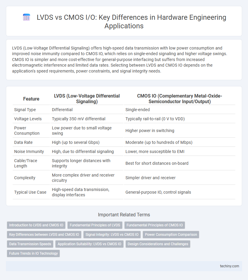
LVDS (Low-Voltage Differential Signaling) offers high-speed data transmission with low power consumption and improved noise immunity compared to CMOS IO, which relies on single-ended signaling and higher voltage swings. CMOS IO is simpler and more cost-effective for general-purpose interfacing but suffers from increased electromagnetic interference and limited data rates. Selecting between LVDS and CMOS IO depends on the application's speed requirements, power constraints, and signal integrity needs.
Table of Comparison
| Feature | LVDS (Low-Voltage Differential Signaling) | CMOS IO (Complementary Metal-Oxide-Semiconductor Input/Output) |
|---|---|---|
| Signal Type | Differential | Single-ended |
| Voltage Levels | Typically 350 mV differential | Typically rail-to-rail (0 V to VDD) |
| Power Consumption | Low power due to small voltage swing | Higher power in switching |
| Data Rate | High (up to several Gbps) | Moderate (up to hundreds of Mbps) |
| Noise Immunity | High, due to differential signaling | Lower, more susceptible to EMI |
| Cable/Trace Length | Supports longer distances with integrity | Best for short distances on-board |
| Complexity | More complex driver and receiver circuitry | Simpler driver and receiver |
| Typical Use Case | High-speed data transmission, display interfaces | General-purpose IO, control signals |
Introduction to LVDS and CMOS IO
LVDS (Low Voltage Differential Signaling) is a high-speed, low-power communication interface commonly used in hardware engineering for transmitting data with minimal electromagnetic interference and signal degradation. CMOS IO (Complementary Metal-Oxide-Semiconductor Input/Output) pins provide versatile, single-ended digital signaling widely employed for general-purpose input and output operations due to their low power consumption and high noise immunity. Understanding the fundamental electrical characteristics and signal integrity aspects of LVDS and CMOS IO enables engineers to optimize interface designs for speed, power efficiency, and reliability in embedded systems and integrated circuits.
Fundamental Principles of LVDS
LVDS (Low-Voltage Differential Signaling) employs differential pairs for data transmission, significantly reducing electromagnetic interference and enabling high-speed communication with low power consumption. Unlike CMOS IO, which uses single-ended signaling and typically operates at higher voltage levels, LVDS achieves better signal integrity by transmitting complementary voltages that minimize noise. This fundamental principle allows LVDS to support data rates exceeding several gigabits per second while maintaining low electromagnetic emissions in hardware designs.
Fundamental Principles of CMOS IO
CMOS IO operates based on complementary pairs of p-type and n-type MOSFETs that switch between full voltage rails, enabling low static power consumption and high noise immunity. Unlike LVDS, which uses differential signaling with constant current for high-speed communication, CMOS IO relies on voltage-driven single-ended signals suited for moderate speed and power efficiency. The fundamental principle of CMOS IO centers on exploiting transistor switching behavior to minimize power dissipation during logic state transitions while maintaining robust digital signal integrity.
Key Differences between LVDS and CMOS IO
LVDS (Low-Voltage Differential Signaling) uses differential signals to achieve high-speed data transmission with low power consumption and reduced electromagnetic interference, while CMOS IO (Complementary Metal-Oxide-Semiconductor Input/Output) relies on single-ended voltage signaling with higher power consumption and slower speed. LVDS offers superior noise immunity and signal integrity over longer distances compared to CMOS IO, which is typically simpler and less expensive for low-speed applications. The key difference lies in LVDS's differential signaling enabling higher data rates and lower noise, versus CMOS IO's single-ended signaling better suited for general-purpose digital input/output.
Signal Integrity: LVDS vs CMOS IO
LVDS (Low-Voltage Differential Signaling) offers superior signal integrity over CMOS IO by using differential signaling that reduces electromagnetic interference (EMI) and crosstalk. LVDS achieves higher noise immunity and lower voltage swings, enabling reliable high-speed data transmission with minimal signal degradation. In contrast, CMOS IO relies on single-ended signaling, making it more susceptible to noise and requiring careful PCB layout to maintain integrity at high frequencies.
Power Consumption Comparison
LVDS (Low-Voltage Differential Signaling) IOs consume significantly lower power compared to CMOS IOs due to their differential signaling and reduced voltage swing, typically operating around 350mV versus the 3.3V or 1.8V of CMOS logic levels. This lower voltage and current requirement translates to decreased dynamic power dissipation, making LVDS ideal for high-speed data transmission with minimal energy use. CMOS IOs, while offering simpler design and higher noise margins, tend to consume more power because of their larger voltage swings and static power leakage in advanced nodes.
Data Transmission Speeds
LVDS (Low-Voltage Differential Signaling) offers significantly higher data transmission speeds compared to CMOS IO, supporting rates upwards of several gigabits per second due to its differential signaling that reduces noise and electromagnetic interference. CMOS IO typically operates at lower speeds, often in the range of hundreds of megabits per second, constrained by single-ended signaling and higher susceptibility to noise. For high-speed data communication in hardware engineering, LVDS is preferred for its superior signal integrity and bandwidth efficiency.
Application Suitability: LVDS vs CMOS IO
LVDS (Low-Voltage Differential Signaling) excels in high-speed data transmission applications requiring low noise and electromagnetic interference, making it suitable for communication interfaces and high-frequency signal processing. CMOS IO (Complementary Metal-Oxide-Semiconductor Input/Output) is ideal for general-purpose digital circuits where low power consumption and simplicity are priorities, often used in microcontrollers and standard digital logic interfaces. The choice between LVDS and CMOS IO depends on the application's speed, signal integrity demands, and power efficiency requirements.
Design Considerations and Challenges
LVDS (Low-Voltage Differential Signaling) offers advantages in high-speed, low-noise data transmission with reduced electromagnetic interference, making it ideal for high-frequency hardware designs. CMOS IO, while simpler and more power-efficient at lower speeds, faces challenges such as higher susceptibility to noise and limited signal integrity over long distances. Designers must weigh trade-offs in power consumption, signal integrity, and board complexity when choosing between LVDS and CMOS IO for hardware systems.
Future Trends in IO Technology
Future trends in IO technology emphasize the increasing adoption of LVDS (Low Voltage Differential Signaling) for its superior noise immunity and high-speed data transfer capabilities compared to traditional CMOS (Complementary Metal-Oxide-Semiconductor) IO. LVDS supports higher bandwidth and lower power consumption, making it ideal for applications in high-performance computing, automotive systems, and advanced communication interfaces. Emerging innovations include integration of LVDS with advanced semiconductor processes and next-generation packaging techniques to enhance signal integrity and scalability.
LVDS vs CMOS IO Infographic