Vias are conductive pathways that connect different layers in a printed circuit board (PCB), passing completely through the board, while blind vias connect outer layers to one or more inner layers without passing all the way through. Blind vias enhance PCB density and signal integrity by reducing the need for through-hole connections and minimizing parasitic capacitance. Choosing between vias and blind vias depends on design complexity, cost constraints, and electrical performance requirements.
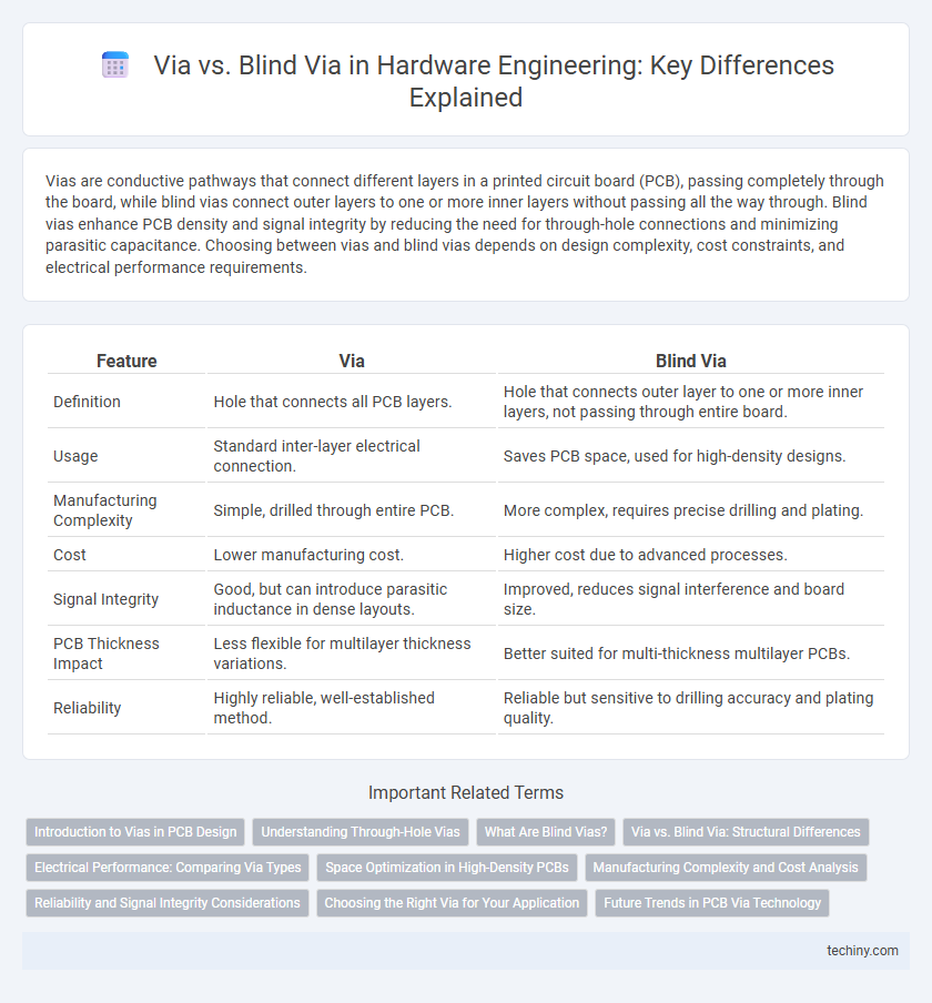
Table of Comparison
| Feature | Via | Blind Via |
|---|---|---|
| Definition | Hole that connects all PCB layers. | Hole that connects outer layer to one or more inner layers, not passing through entire board. |
| Usage | Standard inter-layer electrical connection. | Saves PCB space, used for high-density designs. |
| Manufacturing Complexity | Simple, drilled through entire PCB. | More complex, requires precise drilling and plating. |
| Cost | Lower manufacturing cost. | Higher cost due to advanced processes. |
| Signal Integrity | Good, but can introduce parasitic inductance in dense layouts. | Improved, reduces signal interference and board size. |
| PCB Thickness Impact | Less flexible for multilayer thickness variations. | Better suited for multi-thickness multilayer PCBs. |
| Reliability | Highly reliable, well-established method. | Reliable but sensitive to drilling accuracy and plating quality. |
Introduction to Vias in PCB Design
Vias are essential conductive pathways in PCB design that connect different layers, enabling multi-layer circuit functionality. Blind vias specifically connect outer layers to one or more inner layers without extending through the entire board, optimizing space and signal integrity. Their strategic use enhances electrical performance by minimizing parasitic elements and improving routing density in complex hardware engineering projects.
Understanding Through-Hole Vias
Through-hole vias serve as essential electrical connections by passing completely through a printed circuit board (PCB), enabling signal and power transmission between different layers. Blind vias, in contrast, connect outer layers to one or more inner layers without extending through the entire board, optimizing space in high-density PCB designs. Understanding the differences in via types is crucial for effective hardware engineering, ensuring proper signal integrity and manufacturing cost efficiency.
What Are Blind Vias?
Blind vias are specific types of vias used in printed circuit boards (PCBs) that connect an outer layer to one or more inner layers without passing completely through the board. Unlike through vias, which span the entire PCB thickness, blind vias only penetrate partway, reducing signal interference and preserving board real estate. These vias are essential in high-density interconnect (HDI) designs for enhancing electrical performance and enabling more complex multilayer PCB architectures.
Via vs. Blind Via: Structural Differences
A standard via is a plated hole that connects all the layers of a PCB, running through the entire board, while a blind via only connects an outer layer to one or more inner layers without passing through the entire board. Blind vias enhance board density and signal integrity by minimizing interference and saving space, crucial in multilayer PCBs with complex circuits. Structural differences include via depth, diameter, and fabrication processes where blind vias require precise drilling and plating to maintain electrical performance within targeted layers.
Electrical Performance: Comparing Via Types
Blind vias improve electrical performance by reducing signal path length and minimizing parasitic inductance compared to through-hole vias. These vias enhance high-frequency signal integrity by limiting signal reflection and crosstalk in multilayer PCBs. Choosing blind vias supports faster signal transmission and better overall circuit reliability in advanced hardware designs.
Space Optimization in High-Density PCBs
Blind vias connect outer layers to one or more inner layers without passing through the entire PCB, maximizing space utilization in high-density designs by reducing unnecessary drilling. Via-in-pad technology enables placement of blind vias directly under components, further saving valuable board real estate. This approach enhances signal integrity and allows for tighter routing, crucial for complex, multi-layer hardware engineering projects.
Manufacturing Complexity and Cost Analysis
Blind vias involve drilling from one surface of the PCB to an inner layer without passing through the entire board, increasing manufacturing complexity due to precise depth control requirements and higher risk of defects. Via fabrication generally lowers production costs since they pass completely through the board, simplifying drilling and inspection processes. The added precision and specialized equipment for blind vias result in higher manufacturing costs and longer production times compared to conventional vias.
Reliability and Signal Integrity Considerations
Blind vias enhance signal integrity by minimizing signal path lengths and reducing parasitic capacitance compared to through-hole vias. Reliability improves as blind vias limit stress concentration in the PCB stack-up, lowering the risk of delamination and via barrel cracking. Design choices between via and blind via depend on balancing manufacturing complexity with the need for high-frequency signal performance and long-term durability.
Choosing the Right Via for Your Application
Choosing the right via is critical for optimizing signal integrity and manufacturing cost in hardware engineering. Blind vias connect outer layers to one or more inner layers without passing through the entire board, reducing parasitic capacitance and improving high-frequency performance in dense multilayer PCBs. Via selection depends on factors such as board complexity, layer count, and electrical requirements, with blind vias preferred for minimizing signal loss and through vias favored for simpler, cost-effective designs.
Future Trends in PCB Via Technology
Future trends in PCB via technology emphasize the evolution of blind vias, which offer enhanced signal integrity and miniaturization advantages over traditional through-hole vias by connecting only specific layers, reducing parasitic capacitance and improving high-frequency performance. Advancements in laser drilling and microvia fabrication enable increasingly precise, smaller blind vias that support higher component density and multilayer boards typical in 5G and advanced computing applications. The continued development of materials and manufacturing techniques will drive the adoption of blind vias as a standard, optimizing PCB reliability and electrical performance in next-generation hardware designs.
Via vs Blind via Infographic