Plated Through Holes (PTH) provide reliable electrical connections through multiple layers of a printed circuit board, offering mechanical strength for mounting components, while Via-in-Pad technology integrates vias directly within component pads to save space and improve signal integrity in high-density designs. PTHs are ideal for robust through-hole components and heavy current-carrying paths, whereas via-in-pad is favored in high-speed circuits requiring minimized via inductance and enhanced thermal management. Selecting between PTH and via-in-pad depends on design requirements such as assembly processes, electrical performance, and board manufacturability.
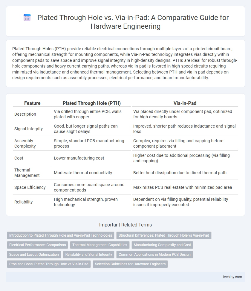
Table of Comparison
| Feature | Plated Through Hole (PTH) | Via-in-Pad |
|---|---|---|
| Description | Via drilled through entire PCB, walls plated with copper | Via placed directly under component pad, optimized for high-density boards |
| Signal Integrity | Good, but longer signal paths can cause slight delays | Improved, shorter path reduces inductance and signal loss |
| Assembly Complexity | Simple, standard PCB manufacturing process | Complex, requires via filling and capping before component placement |
| Cost | Lower manufacturing cost | Higher cost due to additional processing (via filling and capping) |
| Thermal Management | Moderate thermal conductivity | Better heat dissipation due to direct thermal path |
| Space Efficiency | Consumes more board space around component pads | Maximizes PCB real estate with minimized pad area |
| Reliability | High mechanical strength, proven technology | Dependent on via filling quality, potential reliability issues if improperly executed |
Introduction to Plated Through Hole and Via-in-Pad Technologies
Plated Through Hole (PTH) technology involves drilling holes through the PCB and plating them with conductive material to create electrical connections between layers, offering robust mechanical strength and reliable signal integrity for components with leads. Via-in-Pad technology places vias directly within component pads, enabling higher component density and improved electrical performance by reducing parasitic inductance and signal path lengths. Both methods serve critical roles in advanced PCB design, balancing manufacturability, electrical characteristics, and assembly requirements.
Structural Differences: Plated Through Hole vs Via-in-Pad
Plated Through Holes (PTH) are cylindrical holes drilled through the entire PCB layer stack and plated with conductive material to provide electrical connections between different layers, featuring a uniform wall thickness for robust mechanical and electrical reliability. Via-in-Pad technology embeds vias directly within component pads, minimizing signal path lengths and improving high-frequency performance but requiring careful thermal and solder mask management due to potential for solder wicking and pad stress. The primary structural difference lies in PTH's through-layer plating versus Via-in-Pad's localized micro via integration within surface mount pads, impacting manufacturing complexity and circuit density.
Electrical Performance Comparison
Plated Through Holes (PTH) provide reliable electrical connections with low resistance and robust mechanical strength, suitable for high-current applications in hardware engineering. Via-in-Pad technology minimizes signal path length and parasitic inductance, enhancing high-frequency performance and reducing signal loss in dense PCB layouts. Electrical performance comparison shows Via-in-Pad excels in signal integrity and impedance control, while PTH offers better thermal dissipation and current carrying capacity.
Thermal Management Capabilities
Plated Through Hole (PTH) technology offers enhanced thermal dissipation by providing a direct conductive path through the PCB, efficiently transferring heat away from components. Via-in-Pad design improves thermal management by minimizing the thermal resistance between the component pad and the internal layers, enabling better heat conduction in high-density boards. Both methods optimize heat flow, but PTH is generally preferred for heavier components requiring robust thermal performance, while via-in-pad suits fine-pitch applications with stringent space constraints.
Manufacturing Complexity and Cost
Plated Through Hole (PTH) technology involves drilling holes through the entire PCB thickness and plating each hole, which increases manufacturing complexity and cost due to longer processing times and higher material usage. Via-in-Pad integrates vias within component pads, offering reduced signal inductance and miniaturization but requires precise laser drilling and via filling, significantly raising fabrication difficulty and expenses. Choosing between PTH and Via-in-Pad hinges on balancing electrical performance benefits against the increased manufacturing complexity and cost constraints.
Space and Layout Optimization
Plated Through Holes (PTH) consume significant board space due to their larger drill sizes and annular ring requirements, limiting component density in high-density PCB layouts. Via-in-Pad technology offers superior space optimization by embedding vias directly within component pads, reducing signal path lengths and improving electrical performance. This layout optimization enables more compact designs, crucial for miniaturized hardware engineering applications where every millimeter of PCB real estate matters.
Reliability and Signal Integrity
Plated Through Holes (PTH) provide robust mechanical strength and reliable electrical connections, making them suitable for high-current applications, whereas Via-in-Pad designs improve signal integrity by minimizing parasitic inductance and capacitance, essential for high-speed circuits. Via-in-Pad requires careful thermal management to avoid solder joint fatigue, while PTH offers better thermal dissipation and mechanical stability. Selecting between PTH and Via-in-Pad depends on prioritizing reliability in power delivery versus optimizing signal integrity in high-frequency signal paths.
Common Applications in Modern PCB Design
Plated Through Holes (PTH) are commonly used in modern PCB design for mounting components that require robust mechanical support and reliable electrical connections across multiple layers, such as connectors, large passive components, and through-hole ICs. Via-in-Pad technology is favored in high-density PCB designs, especially in advanced packaging and high-frequency applications, as it minimizes signal path length and improves electrical performance by placing vias directly under component pads. Both techniques optimize space and performance but are selected based on design requirements, thermal management, and signal integrity considerations.
Pros and Cons: Plated Through Hole vs Via-in-Pad
Plated Through Hole (PTH) technology offers robust mechanical strength and reliable electrical connections, ideal for high-current components but requires more PCB space and longer manufacturing times. Via-in-Pad enables higher component density and shorter signal paths, enhancing electrical performance for high-frequency designs, yet it poses challenges like increased risk of solder wicking and more complex fabrication processes. Selecting between PTH and Via-in-Pad depends on balancing mechanical stability, electrical requirements, and PCB layout constraints in hardware engineering projects.
Selection Guidelines for Hardware Engineers
Plated Through Hole (PTH) is preferred for components requiring robust mechanical strength and high current capacity, making it ideal for connectors and heavy components. Via-in-Pad is beneficial for high-density PCB layouts, reducing signal path lengths and improving high-frequency performance but demands careful thermal management to avoid soldering issues. Hardware engineers should weigh factors like signal integrity, assembly process compatibility, and mechanical reliability when selecting between PTH and Via-in-Pad techniques.
Plated Through Hole vs Via-in-Pad Infographic