JTAG and SWD are two protocols used for debugging and programming microcontrollers, with JTAG offering a comprehensive interface supporting multiple devices, making it suitable for complex systems. SWD, or Serial Wire Debug, provides a streamlined two-pin interface that reduces pin count and board complexity, ideal for ARM Cortex-M based microcontrollers. Choosing between JTAG and SWD depends on the required debug capabilities, hardware constraints, and specific application needs.
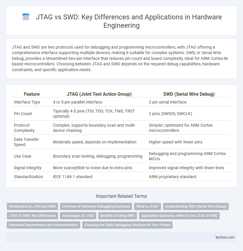
Table of Comparison
| Feature | JTAG (Joint Test Action Group) | SWD (Serial Wire Debug) |
|---|---|---|
| Interface Type | 4 or 5-pin parallel interface | 2-pin serial interface |
| Pin Count | Typically 4-5 pins (TDI, TDO, TCK, TMS, TRST optional) | 2 pins (SWDIO, SWCLK) |
| Protocol Complexity | Complex; supports boundary scan and multi-device chaining | Simpler; optimized for ARM Cortex microcontrollers |
| Data Transfer Speed | Moderate speed, depends on implementation | Higher speed with fewer pins |
| Use Case | Boundary scan testing, debugging, programming | Debugging and programming ARM Cortex MCUs |
| Signal Integrity | More susceptible to noise due to extra pins | Improved signal integrity with fewer lines |
| Standardization | IEEE 1149.1 standard | ARM proprietary standard |
Introduction to JTAG and SWD
JTAG (Joint Test Action Group) is a widely used hardware interface standard for testing and debugging integrated circuits through boundary-scan architecture, enabling access to device internals without physical probes. SWD (Serial Wire Debug) offers a streamlined, two-pin interface for ARM Cortex processors, providing efficient debugging and programming with reduced pin count compared to JTAG's multi-pin setup. Both protocols support in-circuit debugging and programming, but SWD is favored in low-pin-count, power-sensitive embedded systems due to its simplicity and lower overhead.
Overview of Hardware Debugging Interfaces
JTAG (Joint Test Action Group) and SWD (Serial Wire Debug) are essential hardware debugging interfaces used in embedded system development for accessing and controlling microcontroller internals. JTAG supports a multi-pin interface enabling boundary-scan testing, device programming, and complex debugging tasks, often used in FPGAs and complex SoCs. SWD, a two-wire protocol alternative to JTAG for ARM Cortex-M processors, provides efficient debugging and programming with reduced pin count, optimizing board design and space in embedded systems.
What is JTAG?
JTAG (Joint Test Action Group) is a standard interface used for verifying designs and testing printed circuit boards after manufacture by providing access to the boundary scan architecture of integrated circuits. It enables debugging, programming, and device identification through a standardized 4- or 5-pin serial communication interface. Widely adopted in hardware engineering, JTAG supports complex systems by allowing direct control of chips for fault detection and in-system programming.
Understanding SWD (Serial Wire Debug)
Serial Wire Debug (SWD) is a two-pin interface designed as a low-pin-count alternative to JTAG for debugging ARM Cortex-M microcontrollers. SWD utilizes a clock line (SWCLK) and a single bi-directional data line (SWDIO) to facilitate efficient on-chip debugging and programming. Its streamlined protocol reduces hardware complexity while maintaining robust debugging capabilities, making it ideal for compact embedded system designs.
JTAG vs SWD: Key Differences
JTAG (Joint Test Action Group) interfaces typically support boundary scan testing and debugging for multiple devices in a chain, offering extensive device control and standardized access to internal registers. SWD (Serial Wire Debug) uses fewer pins and is optimized for ARM Cortex processors, providing a high-speed, two-wire debug protocol primarily focused on programming and debugging with lower pin count and reduced complexity. The key differences lie in the pin requirements, protocol complexity, device support scope, and usage scenarios where JTAG suits multi-device environments and SWD favors streamlined ARM debugging.
Advantages of JTAG
JTAG offers comprehensive debugging capabilities with multi-core support, enabling boundary scan testing and in-system programming for complex hardware designs. Its standardized interface facilitates broad compatibility across various semiconductor devices, enhancing debugging precision and efficiency. The ability to test interconnects and perform fault isolation without powering up the system distinguishes JTAG as a critical tool in hardware validation and manufacturing.
Benefits of Using SWD
SWD (Serial Wire Debug) offers significant benefits in hardware engineering by providing a simpler, two-pin interface compared to JTAG's multiple-pin configuration, reducing PCB complexity and cost. Its efficient use of pins enables easier access to ARM Cortex-M processors for debugging and programming while maintaining high-speed data transfer and control. SWD also supports advanced features like breakpoint and watchpoint management, increasing development productivity and improving firmware debugging accuracy.
Application Scenarios: When to Use JTAG or SWD
JTAG is preferred in complex hardware debugging, boundary scan testing, and multi-device programming due to its standardized interface and support for multiple devices on a single chain. SWD excels in low-pin-count microcontroller debugging and flash programming, offering faster communication with reduced PCB complexity, ideal for resource-constrained embedded systems. Selecting JTAG or SWD depends on factors like device architecture, debug port availability, and the need for advanced test features or streamlined connectivity.
Hardware Requirements and Implementation
JTAG (Joint Test Action Group) interfaces require more pins, typically four to five, including TCK, TMS, TDI, TDO, and optional TRST, which increases board complexity and routing challenges compared to SWD (Serial Wire Debug), which uses only two pins, SWDIO and SWCLK, reducing hardware overhead. Implementation of JTAG involves a more complex state machine and signal coordination, demanding FPGA or dedicated hardware controllers, while SWD is designed for simpler microcontroller access with less intricate timing control, enabling streamlined firmware integration. SWD's minimal pin requirement and simpler protocol make it preferable for compact designs and cost-sensitive applications where PCB space and pin count are constrained.
Choosing the Right Debugging Interface for Your Project
JTAG and SWD are essential debugging interfaces in hardware engineering, with JTAG offering multi-device chain support and broad industry compatibility, ideal for complex systems requiring boundary scan testing. SWD provides a streamlined, two-pin interface that reduces pin count and power consumption, making it optimal for resource-constrained microcontroller projects. Selecting the right interface depends on project requirements such as device complexity, available pins, and debugging depth, ensuring efficient development and troubleshooting.
JTAG vs SWD Infographic