Ground plane and ground fill serve different purposes in hardware engineering; a ground plane is a continuous layer of copper connected to the ground, providing low impedance paths and minimizing electromagnetic interference (EMI). Ground fill refers to areas of copper poured around components and traces, which enhances thermal dissipation and reduces noise but may introduce ground loops if not properly connected to the main ground plane. Optimizing the balance between ground plane and ground fill improves signal integrity and overall circuit performance.
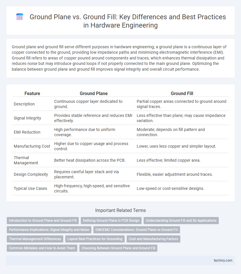
Table of Comparison
| Feature | Ground Plane | Ground Fill |
|---|---|---|
| Description | Continuous copper layer dedicated to ground. | Partial copper areas connected to ground around signal traces. |
| Signal Integrity | Provides stable reference and reduces EMI effectively. | Less effective than plane; may cause impedance variation. |
| EMI Reduction | High performance due to uniform coverage. | Moderate; depends on fill pattern and connection. |
| Manufacturing Cost | Higher due to copper usage and process control. | Lower, uses less copper and simpler layout. |
| Thermal Management | Better heat dissipation across the PCB. | Less effective; limited copper area. |
| Design Complexity | Requires careful layer stack and via placement. | Flexible, easier adjustment around traces. |
| Typical Use Cases | High-frequency, high-speed, and sensitive circuits. | Low-speed or cost-sensitive designs. |
Introduction to Ground Plane and Ground Fill
A ground plane is a continuous layer of copper on a printed circuit board (PCB) that serves as a common reference point for all electrical signals, enhancing signal integrity and reducing electromagnetic interference (EMI). Ground fill refers to sections of copper poured around the components and traces on a PCB, connected to the ground plane to improve grounding efficiency and thermal management. Both ground plane and ground fill are essential in minimizing noise, stabilizing voltage levels, and improving overall PCB performance in hardware engineering.
Defining Ground Plane in PCB Design
A ground plane in PCB design is a continuous layer of copper on one or more layers dedicated to electrical grounding, providing a low-impedance path to reduce noise and interference. It enhances signal integrity by minimizing electromagnetic interference (EMI) and preventing ground loops, crucial for high-frequency and sensitive circuits. Unlike ground fill, which is scattered copper areas connected to ground, a ground plane offers consistent and comprehensive grounding coverage across the PCB.
Understanding Ground Fill and Its Applications
Ground fill refers to the practice of filling unused PCB areas with copper connected to the ground plane to enhance electromagnetic compatibility (EMC) and reduce signal noise. It improves thermal dissipation by providing a larger copper area for heat spreading and minimizes voltage fluctuations across the ground plane by lowering ground impedance. Ground fill is commonly applied in high-speed digital and RF circuits where maintaining a stable reference ground and controlling EMI is critical.
Performance Implications: Signal Integrity and Noise
Ground planes provide a continuous low-impedance reference that enhances signal integrity by minimizing voltage fluctuations and reducing electromagnetic interference (EMI). Ground fills, while easier to implement, may introduce impedance discontinuities and increase noise susceptibility due to fragmented grounding paths. Effective hardware engineering demands careful selection between ground plane and ground fill strategies to optimize noise reduction and maintain consistent signal performance.
EMI/EMC Considerations: Ground Plane vs Ground Fill
Ground planes offer superior EMI/EMC performance by providing a low-impedance return path and minimizing loop area, which reduces electromagnetic interference and improves signal integrity. Ground fills can be effective in partitioning signal layers and controlling impedance but may introduce noise coupling due to their segmented nature, potentially compromising EMC compliance. Optimizing PCB design with continuous ground planes rather than broken fills enhances shielding effectiveness and lowers radiated emissions in high-speed hardware engineering.
Thermal Management Differences
Ground planes provide continuous copper areas that efficiently dissipate heat across the PCB, reducing hotspots and maintaining thermal stability in high-power circuits. Ground fills, by contrast, are segmented copper regions that offer less uniform heat distribution, often resulting in localized thermal buildup and reduced overall conductivity. Effective thermal management in hardware engineering favors ground planes for their superior heat spreading capabilities, crucial in minimizing thermal stress and enhancing component reliability.
Layout Best Practices for Grounding
Ground plane provides a continuous, low-impedance path essential for signal integrity and EMI reduction in PCB design, while ground fill serves as a supplemental grounding method filling unused areas. Best practices prioritize a solid, uninterrupted ground plane layer directly beneath signal traces to minimize inductive loops and maintain consistent reference potential. Effective grounding layout combines extensive ground planes with strategically placed ground fills connected through multiple vias to enhance current return paths and reduce noise coupling.
Cost and Manufacturing Factors
Ground planes reduce manufacturing complexity by providing a uniform reference layer, which lowers production costs through simplified layer stack-up and consistent impedance control. Ground fills, often used in PCB design to economize copper usage, can introduce additional etching steps and potential signal integrity issues, potentially increasing manufacturing expenses. Selecting between a solid ground plane and ground fill depends on balancing material savings with the impact on fabrication yield, electromagnetic compatibility, and overall production efficiency.
Common Mistakes and How to Avoid Them
Ground plane design errors often stem from inconsistent layer usage or insufficient copper coverage, causing signal integrity issues and increased EMI. Ground fill mistakes include improper isolation from sensitive analog circuits and incorrect thermal reliefs, leading to noise coupling and heat dissipation problems. Ensuring continuous, unbroken ground planes with strategic fills and proper clearance zones significantly mitigates return path disruptions and electromagnetic interference.
Choosing Between Ground Plane and Ground Fill
Choosing between a ground plane and ground fill in hardware engineering depends on signal integrity requirements and PCB design complexity. A ground plane offers a continuous, low-impedance return path ideal for high-frequency circuits, reducing EMI and improving noise immunity. Ground fill is suitable for less critical sections where cost savings and easier routing are prioritized, but it may introduce higher impedance and potential noise issues.
Ground Plane vs Ground Fill Infographic