Leaded packages in hardware engineering offer reliable soldering and ease of repair but pose environmental and health risks due to toxic materials like lead. Lead-free packages comply with RoHS standards, promoting sustainability and reducing hazardous waste, though they often require higher soldering temperatures and can present challenges in manufacturing consistency. Choosing between leaded and lead-free packages depends on balancing regulatory compliance, environmental impact, and production requirements.
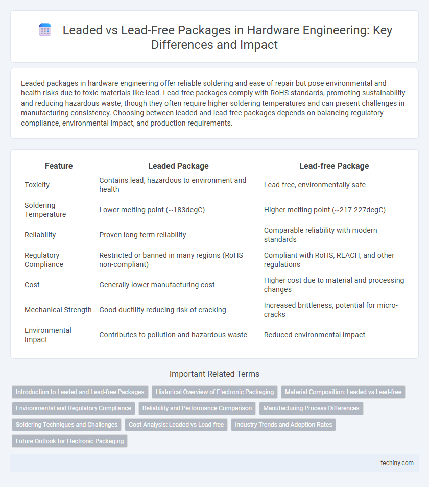
Table of Comparison
| Feature | Leaded Package | Lead-free Package |
|---|---|---|
| Toxicity | Contains lead, hazardous to environment and health | Lead-free, environmentally safe |
| Soldering Temperature | Lower melting point (~183degC) | Higher melting point (~217-227degC) |
| Reliability | Proven long-term reliability | Comparable reliability with modern standards |
| Regulatory Compliance | Restricted or banned in many regions (RoHS non-compliant) | Compliant with RoHS, REACH, and other regulations |
| Cost | Generally lower manufacturing cost | Higher cost due to material and processing changes |
| Mechanical Strength | Good ductility reducing risk of cracking | Increased brittleness, potential for micro-cracks |
| Environmental Impact | Contributes to pollution and hazardous waste | Reduced environmental impact |
Introduction to Leaded and Lead-free Packages
Leaded packages, traditionally used in hardware engineering, contain metallic leads made from alloys including lead, offering reliable solderability and mechanical stability for electronic components. Lead-free packages have emerged due to environmental regulations like RoHS, utilizing alternative alloys such as tin-silver-copper to eliminate toxic lead while maintaining electrical performance. Both package types influence assembly processes, thermal management, and long-term device reliability in electronic manufacturing.
Historical Overview of Electronic Packaging
Leaded packages dominated electronic packaging from the 1950s through the early 2000s, providing reliable mechanical connections and ease of assembly with tin-lead solder alloys. The industry shifted toward lead-free packages due to environmental regulations like RoHS (Restriction of Hazardous Substances) implemented in the early 2000s, driving innovation in materials and soldering techniques. Lead-free packages utilize alloys such as SAC (tin-silver-copper) to meet performance standards while reducing toxic lead content in electronics manufacturing.
Material Composition: Leaded vs Lead-free
Leaded packages primarily consist of tin-lead alloy solder, which offers excellent electrical conductivity and mechanical strength but poses environmental and health risks due to lead content. Lead-free packages replace lead with alternative materials such as tin-silver-copper (SAC) alloys, enhancing environmental safety while maintaining reliable solder joint performance under thermal stress. The shift from leaded to lead-free compositions aligns with RoHS (Restriction of Hazardous Substances) regulations, emphasizing sustainable manufacturing practices in hardware engineering.
Environmental and Regulatory Compliance
Leaded packages, containing hazardous substances like lead, face increasing restrictions under environmental regulations such as RoHS and REACH, compelling manufacturers to adopt lead-free alternatives. Lead-free packages utilize tin, silver, and copper alloys, significantly reducing toxic waste and improving recyclability in electronic components. Compliance with global directives ensures safer disposal practices, minimizing environmental impact while supporting sustainable hardware engineering practices.
Reliability and Performance Comparison
Leaded packages offer superior solder joint reliability under thermal cycling due to their ductile tin-lead alloy, which reduces crack propagation and enhances mechanical stability in harsh environments. Lead-free packages utilize tin-silver-copper (SAC) alloys that provide higher melting points and improved environmental compliance but often exhibit increased brittleness, leading to potential micro-cracking and reduced long-term reliability. Performance-wise, leaded packages maintain consistent electrical conductivity and thermal performance, while lead-free options may experience slightly higher contact resistance and thermal stress, impacting overall device durability in demanding hardware engineering applications.
Manufacturing Process Differences
Leaded packages typically involve through-hole mounting with solder joints formed by dipping leads into molten solder, allowing for robust mechanical and electrical connections, while lead-free packages use surface-mount technology (SMT) with solder paste reflow, requiring precise temperature profiles due to higher melting points of lead-free alloys like SAC305. The lead-free manufacturing process demands stricter thermal management to prevent component damage and ensure reliability, often incorporating advanced fluxes and extended preheat stages. These differences influence equipment calibration, process control, and compliance with environmental regulations such as RoHS.
Soldering Techniques and Challenges
Leaded packages utilize solder alloys containing lead, which provide a lower melting point and better wettability, simplifying soldering processes and reducing the risk of thermal damage to components. Lead-free packages require higher soldering temperatures due to their tin-silver-copper compositions, increasing challenges such as component stress, solder joint reliability, and the need for precise thermal management. The industry's shift to lead-free soldering demands advanced assembly techniques like reflow profiling optimization and flux formulation improvements to ensure strong, defect-free joints in electronic hardware.
Cost Analysis: Leaded vs Lead-free
Leaded packages generally incur higher material costs due to the use of hazardous substances requiring stringent handling and disposal procedures, impacting overall manufacturing expenses. Lead-free packages, while often more expensive in initial production due to advanced alloy materials and specialized processing techniques, reduce long-term costs by complying with environmental regulations such as RoHS and minimizing health-related liabilities. Cost analysis also factors in yield rates, as lead-free solder can present challenges in reliability and rework, potentially increasing manufacturing time and expense.
Industry Trends and Adoption Rates
Leaded packages have historically dominated hardware engineering due to their reliable solderability and mechanical strength, but industry trends increasingly favor lead-free packages driven by stringent environmental regulations such as RoHS and REACH. Adoption rates of lead-free packages have surged in sectors like consumer electronics and automotive, where sustainability and compliance are critical, reaching over 85% penetration in new product designs by 2024. Advances in lead-free solder alloys and improved thermal performance support this transition, making lead-free solutions the industry standard while leaded packages remain in niche or legacy applications.
Future Outlook for Electronic Packaging
The future outlook for electronic packaging indicates a strong shift towards lead-free packages driven by stringent environmental regulations like RoHS and increasing demand for sustainable electronics. Lead-free packages, such as those using tin-silver-copper (SAC) alloys, offer improved reliability and compatibility with lead-free PCB finishes, enabling higher operating temperatures and enhanced solder joint durability. Despite legacy systems relying on leaded packages due to their superior wetting properties and lower melting points, emerging innovations in lead-free materials are expected to dominate the market, promoting eco-friendly manufacturing and compliance with global standards.
Leaded Package vs Lead-free Package Infographic